Semiconductor manufacturing apparatus and semiconductor manufacturing method

a manufacturing apparatus and semiconductor technology, applied in the field of wet processing technique, can solve the problems of increasing the consumption of stock solutions, the in-plane uniformity of chemical liquid processes, and the need to increase the quantity of additional supplies, so as to achieve the effect of increasing the diameter and sufficient in-plane uniformity

Active Publication Date: 2022-01-18
MITSUBISHI ELECTRIC CORP
View PDF12 Cites 0 Cited by
  • Summary
  • Abstract
  • Description
  • Claims
  • Application Information

AI Technical Summary

Benefits of technology

[0010]It is an object of the present invention to provide a technique that allows sufficient in-plane uniformity in a chemical liquid process to be ensured even within a range of an operation condition where a physical limit becomes severe due to, for example, an increase in diameter of a wafer.
[0011]A semiconductor manufacturing apparatus according to the present invention includes a chuck stage, a stage rotation mechanism, a chemical liquid nozzle, a chemical liquid nozzle scan mechanism, a gas nozzle, a gas temperature controller, a gas bypass pipe, and an on-off valve. The chuck stage holds a wafer using an end portion of the chuck stage. The stage rotation mechanism rotates the chuck stage. The chemical liquid nozzle discharges a chemical liquid to a processing surface of the wafer. The chemical liquid nozzle scan mechanism causes the chemical liquid nozzle to perform a scan on the processing surface of the wafer. The gas nozzle supplies gas to an opposite surface opposed to the processing surface of the wafer. The gas temperature controller controls a temperature of the gas to be supplied to the gas nozzle. The gas bypass pipe allows the gas to be supplied the gas nozzle without causing the gas to pass through the gas temperature controller. The on-off valve opens and shuts to allow either of the gas whose temperature has been controlled by the gas temperature controller and the gas passing through the gas bypass pipe to be supplied to the gas nozzle. Actuation of the on-off valve allows a temperature of the gas passing through the gas nozzle to be changed.
[0012]Since the chemical liquid process can be performed with a temperature uniform all over the wafer, in-plane uniformity in the chemical liquid process can be sufficiently ensured.

Problems solved by technology

However, when there is a physical limit to a range of an operation condition, the effect is also limited, and as a result, in-plane uniformity in the chemical liquid process is also limited.
Further, the increase in the flow rate of the chemical liquid increases the pace of volatilization and decomposition of chemical liquid components contained in the chemical liquid, so that a stock solution to be additionally supplied needs to be increased and is accordingly increased in consumption.
Further, in a supply-controlled chemical liquid process such as etching of an Si wafer with fluoro-nitric acid, it is not sufficient to spread the chemical liquid on the upper surface of the wafer uniformly all over the upper surface of the wafer, and it is necessary to ensure that the chemical liquid is uniformly activated all over the upper surface of the wafer.
However, when there are physical limits to the ranges of the operation conditions, the optimization also becomes insufficient.
In particular, in a case of a chemical liquid process such as etching of an Si wafer with fluoro-nitric acid where reaction heat is generated, it fails to take a measure such as giving rise to, in the area around the center portion of the wafer, a reaction appropriate to a reaction that is liable to occur at the center portion of the wafer and is accelerated or decelerated in accordance with the intensity of activity, and as a result, the in-plane uniformity in the chemical liquid process is also limited.
Further, in the technique described in Japanese Patent Application Laid-Open No. 2005-217226, the wafer is fixed to a mounting table and is directly heated, and temperature unevenness occurs due to poor adhesion between the wafer and the mounting table, which prevents the chemical liquid process from being performed with the temperature uniform all over the wafer, and accordingly makes it difficult to achieve the in-plane uniformity in the chemical liquid process.

Method used


Image

  • Semiconductor manufacturing apparatus and semiconductor manufacturing method
  • Semiconductor manufacturing apparatus and semiconductor manufacturing method
  • Semiconductor manufacturing apparatus and semiconductor manufacturing method

Examples


first preferred embodiment

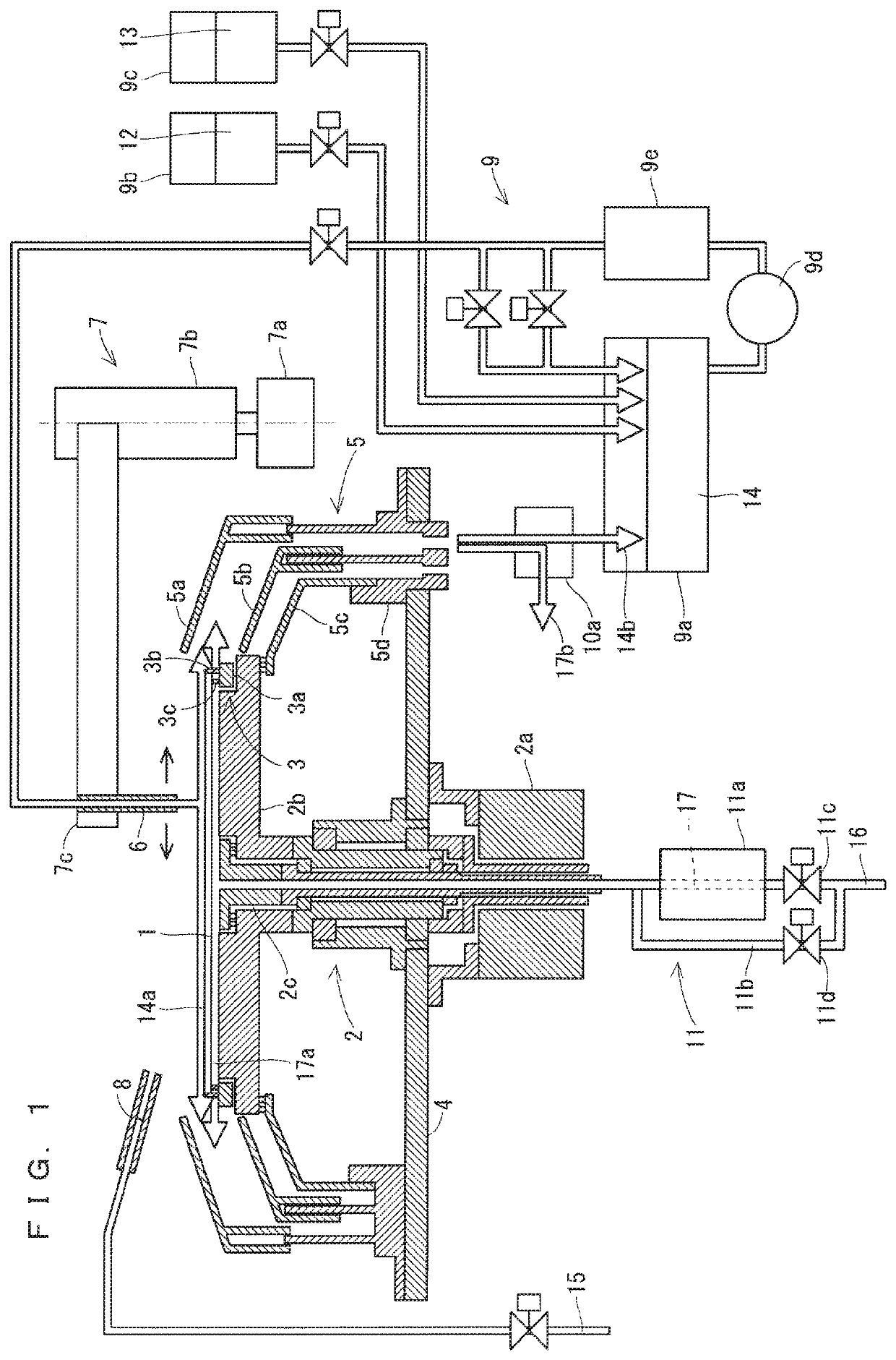
[0053]A description will be given of a first preferred embodiment of the present invention with reference to the drawings. Note that, in the first preferred embodiment, the same components as those described in the underlying technology are denoted by the same reference numerals, and descriptions thereof will be omitted. FIG. 1 is a cross-sectional view showing a chemical liquid process in a processing chamber of a semiconductor manufacturing apparatus according to the first preferred embodiment.

[0054]As shown in FIG. 1, the semiconductor manufacturing apparatus according to the first preferred embodiment further includes a lower surface gas temperature control discharge mechanism 11 in addition to the components of the semiconductor manufacturing apparatus according to the underlying technology shown in FIG. 9. The configuration of the semiconductor manufacturing apparatus according to the first preferred embodiment is substantially the same as the configuration according to the un...

second preferred embodiment

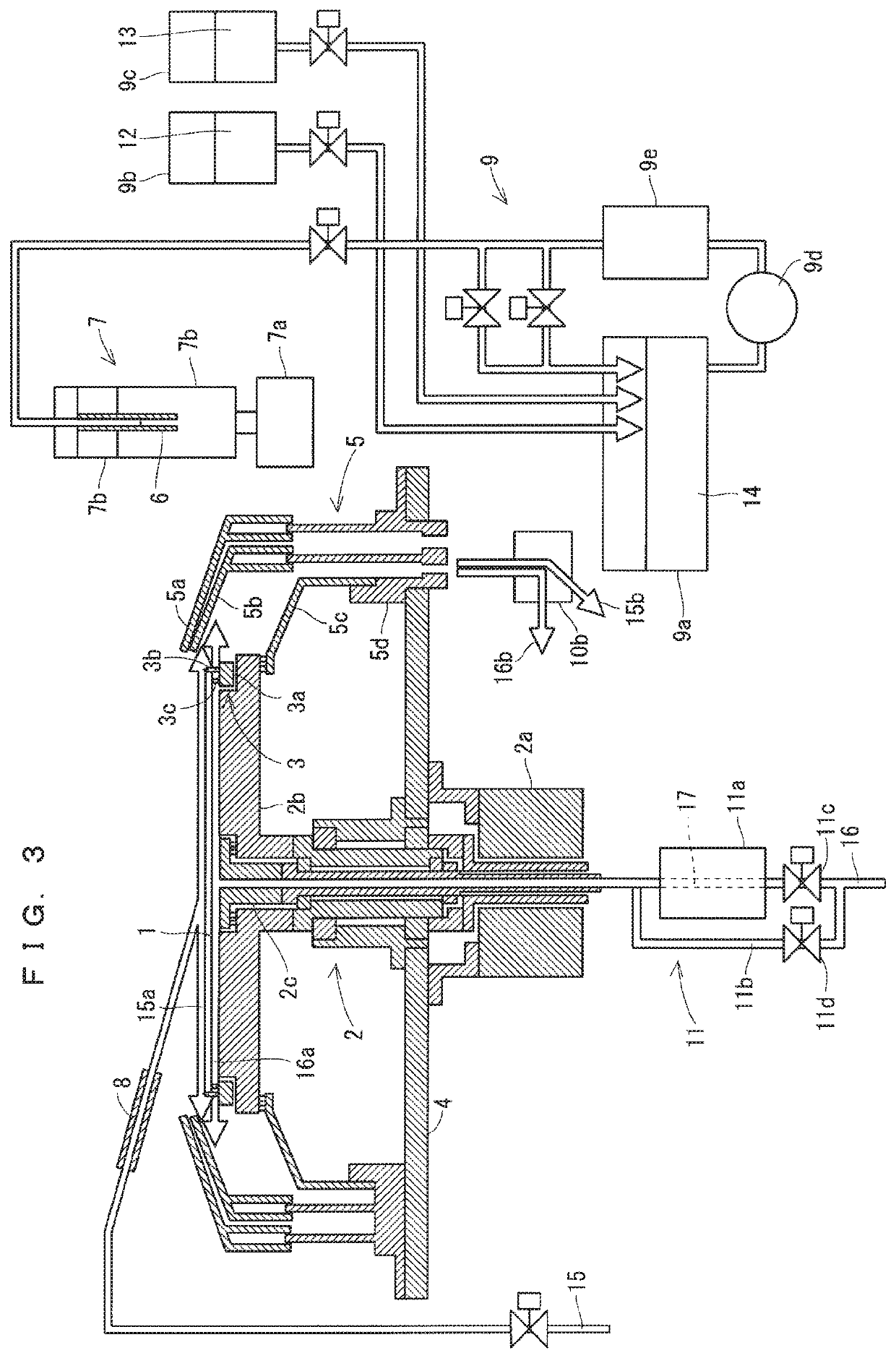
[0084]Next, a description will be given of a semiconductor manufacturing apparatus according to a second preferred embodiment. FIG. 6 is a cross-sectional view showing a chemical liquid process in a processing chamber of the semiconductor manufacturing apparatus according to the second preferred embodiment. Note that, in the second preferred embodiment, the same components as those described in the first preferred embodiment are denoted by the same reference numerals, and descriptions thereof will be omitted.

[0085]As shown in FIG. 6, the semiconductor manufacturing apparatus according to the second preferred embodiment includes a lower surface gas nozzle 2d instead of the lower surface gas nozzle 2c. A discharge port of the lower surface gas nozzle 2d is positioned to surround a center portion of a wafer 1.

[0086]The lower surface gas nozzle 2d is different in structure from the lower surface gas nozzle 2c described in the first preferred embodiment whose discharge port is positioned...


PUM


Abstract

A semiconductor manufacturing apparatus includes a chuck stage, a stage rotation mechanism, a chemical liquid nozzle, a chemical liquid nozzle scan mechanism, a lower surface gas nozzle, a gas temperature controller configured to control a temperature of gas to be supplied to the lower surface gas nozzle, a gas bypass pipe configured to allow the gas to be supplied to the lower surface gas nozzle without causing the gas to pass through the gas temperature controller, and first and second on-off valves configured to open and shut to allow either of the gas whose temperature has been controlled by the gas temperature controller and the gas passing through the gas bypass pipe to be supplied to the lower surface gas nozzle. Actuation of the first and second on-off valves allows a temperature of the gas passing through the lower surface gas nozzle to be changed.

Description

BACKGROUND OF THE INVENTIONField of the Invention[0001]The present invention relates to a wet processing technique implemented by discharging a chemical liquid to a semiconductor wafer.Description of the Background Art[0002]In a semiconductor manufacturing process, after a pattern of organic material is formed by lithography using a resist, etching is performed on an oxide film or a metal material by dry etching using several types of gas energized through application of a high-frequency output.[0003]Thereafter, in order to remove the resist, a chemical liquid is used to dissolve the resist. As a method of removing a resist using a chemical liquid, the technique described in Japanese Patent Application Laid-Open No. 2005-217226 is disclosed, for example.[0004]In a conventional general semiconductor manufacturing apparatus, a chemical liquid process is performed by discharging a chemical liquid at a predetermined flow rate while rotating a semiconductor wafer at a predetermined rotat...

Claims


Application Information

Patent Timeline
Patent Type & Authority Patents(United States)
IPC IPC(8): H01L21/02B08B3/10H01L21/67H01L21/306H01L21/461H01L21/3213
CPCH01L21/02057B08B3/10H01L21/30604H01L21/32134H01L21/461H01L21/6708H01L21/67109H01L21/67248H01L21/67028
Inventor TANAKA, HIROSHI
Owner MITSUBISHI ELECTRIC CORP
Why Eureka
Try Eureka