Dynamic random access memory and method of forming the same

a random access memory and dynamic technology, applied in the field of memory devices, can solve the problems of increasing the complexity reducing the critical dimension of the dram, and increasing the difficulty of the dram process, so as to improve the coupling interference, reduce the parasitic capacitance, and enhance the reliability of the dram

Active Publication Date: 2022-04-05
POWERCHIP SEMICON MFG CORP
View PDF7 Cites 0 Cited by
  • Summary
  • Abstract
  • Description
  • Claims
  • Application Information

AI Technical Summary

Benefits of technology

[0005]The invention provides a dynamic random access memory (DRAM) and a method of forming the same in which can reduce the parasitic capacitance between adjacent bit-line structures, so as to improve the coupling interference between adjacent bit-line structures, thereby enhancing the reliability of the DRAM.
[0016]Based on the above, in the embodiment of the present invention, the air gaps are formed between the bit-line structures to effectively reduce the parasitic capacitance between the bit-line structures, thereby improving the coupling interference between the bit-line structures and enhancing the reliability of the DRAM.

Problems solved by technology

However, under this trend, the critical dimension of the DRAM is also reduced, which result in many challenges for the DRAM process.
For example, as the integration density of the DRAM continues to increase, the crosstalk between the memory cells, i.e., the bit line coupling, becomes more and more serious, thereby affecting the operation of the DRAM.

Method used


Image

  • Dynamic random access memory and method of forming the same
  • Dynamic random access memory and method of forming the same
  • Dynamic random access memory and method of forming the same

Examples


Embodiment Construction

[0023]The invention is more blanketly described with reference to the figures of the present embodiments. However, the invention can also be implemented in various different forms, and is not limited to the embodiments in the present specification. The thicknesses of the layers and regions in the figures are enlarged for clarity. The same or similar reference numerals represent the same or similar devices and are not repeated in the following paragraphs.

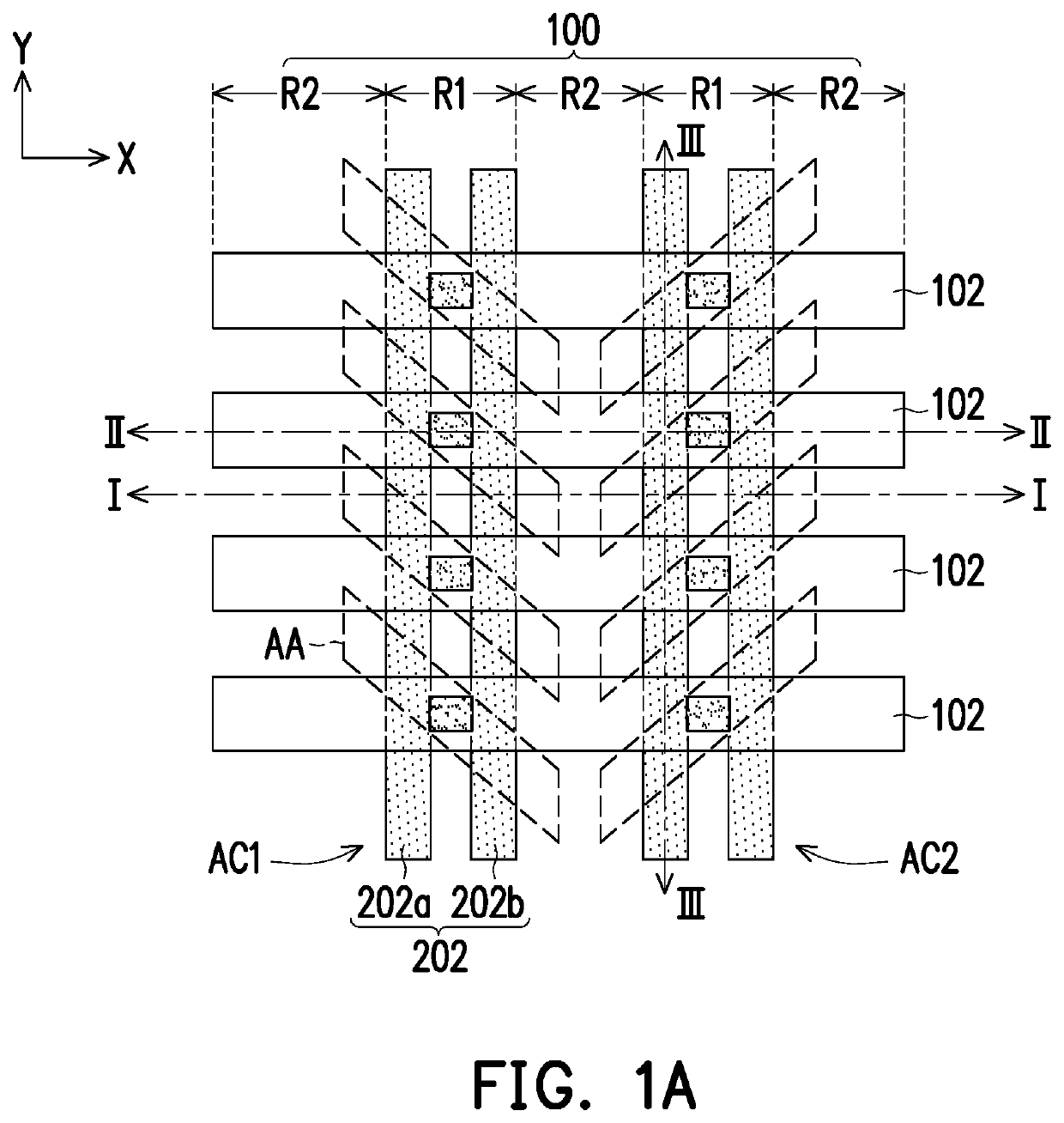
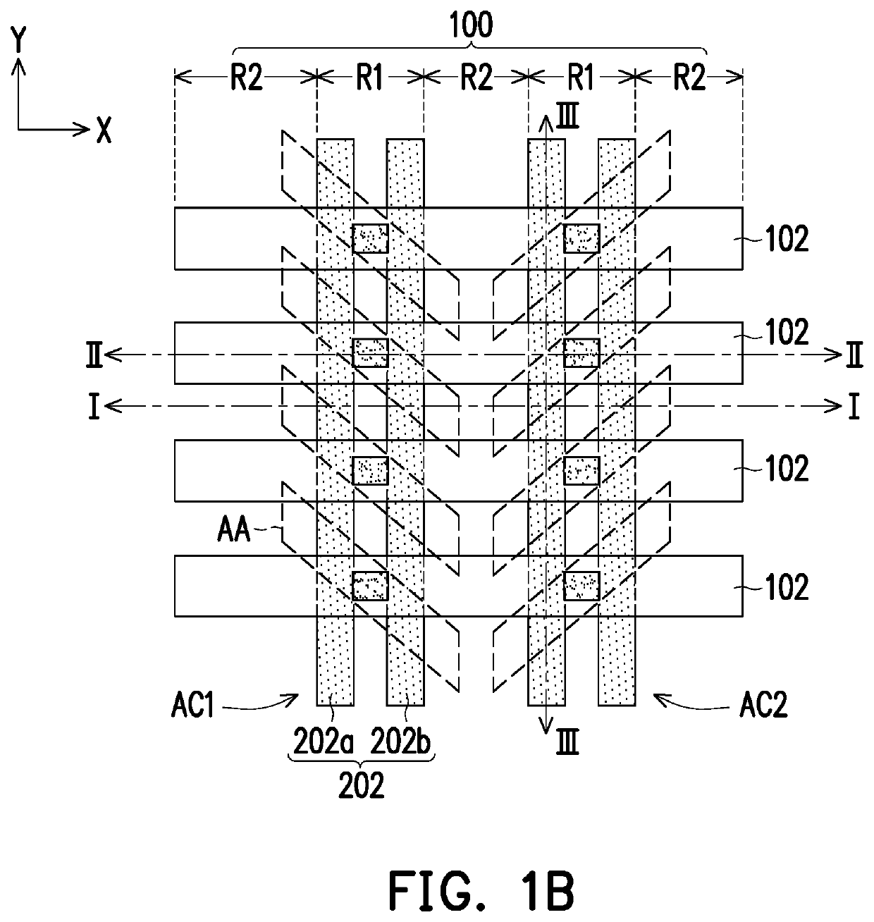
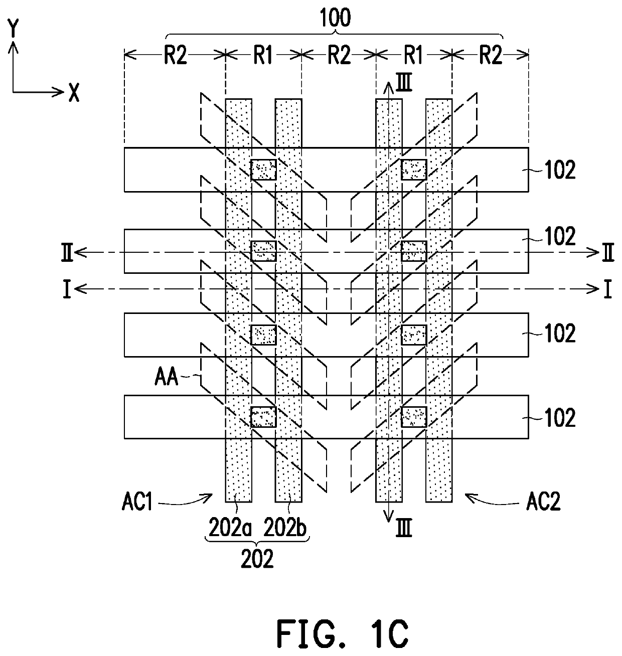
[0024]FIG. 1A to FIG. 1N are schematic top views illustrating a manufacturing process of a memory device according to an embodiment of the invention. FIG. 2A to FIG. 2N are schematic cross-sectional views along line I-I depicted in FIG. 1A to FIG. 1N, respectively. FIG. 3A to FIG. 3N are schematic cross-sectional views along line II-II depicted in FIG. 1A to FIG. 1N, respectively. FIG. 4A to FIG. 4N are schematic cross-sectional views along line III-III depicted in FIG. 1A to FIG. 1N, respectively.

[0025]Referring to FIG. 1A, FIG. 2A,...


PUM


Abstract

Provided is a dynamic random access memory (DRAM) including a substrate, a plurality of word-line sets, a plurality of bit-line structures, a plurality of capacitors, a plurality of capacitor contacts, and a plurality of air gaps. The substrate has a plurality of active areas. The word-line sets extend along a Y direction and disposed in the substrate. The bit-line structures extend along a X direction, disposed on the substrate, and across the word-line sets. The capacitors are respectively disposed at two terminals of the active areas. The capacitor contacts are respectively disposed between the capacitors and the active regions. The air gaps are disposed in a plurality of spaces enclosed by the bit-line structures and the capacitor contacts. A method of forming a DRAM is also provided.

Description

CROSS-REFERENCE TO RELATED APPLICATION[0001]This application claims the priority benefit of Taiwan application serial no. 109128793, filed on Aug. 24, 2020. The entirety of the above-mentioned patent application is hereby incorporated by reference herein and made a part of this specification.BACKGROUND OF THE INVENTIONField of the Invention[0002]The present invention relates to a memory device and a method of forming the same, and more particularly to a dynamic random access memory and a method of forming the same.Description of Related Art[0003]A dynamic random access memory (DRAM) is a volatile memory formed by a plurality of memory cells. Each of the memory cells is mainly composed of a transistor and a capacitor controlled by the transistor, and the memory cells are electrically connected with one another through word lines and bit lines. In order to improve the integration of DRAM to increase the operating speed of the device and to meet the consumers' demand for miniaturizatio...

Claims


Application Information

Patent Timeline
Patent Type & Authority Patents(United States)
IPC IPC(8): H01L27/108H01L21/764H01L21/768
CPCH01L27/10885H01L21/7682H01L27/10814H01L27/10823H01L27/10855H01L27/10876H10B12/30H10B12/03H10B12/48H10B12/485H01L21/76897H01L21/76885H10B12/315H10B12/34H10B12/0335H10B12/482H10B12/053
Inventor CHANG, LI-PENGCHANG, SAN-JUNG
Owner POWERCHIP SEMICON MFG CORP
Why Eureka
Try Eureka