Detector of electromagnetic radiation and in particular infrared radiation, and process for producing said detector

a detector and electromagnetic radiation technology, applied in the field of infrared imaging, can solve the problems of increasing the electric resistance rb, affecting the response of high resistivities, and no longer enabling the guarantee of detector characteristics at a sufficient level, etc., and achieve the effect of increasing the lifetime of the detector

Active Publication Date: 2022-06-14
COMMISSARIAT A LENERGIE ATOMIQUE ET AUX ENERGIES ALTERNATIVES +1
View PDF15 Cites 0 Cited by
  • Summary
  • Abstract
  • Description
  • Claims
  • Application Information

AI Technical Summary

Benefits of technology

[0063]By means of such a material, the Applicants have shown that in the range of temperatures of integration, and thus of closing (sealing) of the package and of getter activation, that is, typically in the range from 280 to 320° C., the resistivity variation of the thermistor material used remains very contained, conversely to materials used in prior art, such a stability providing a satisfactory uniformity of the resulting signal at the readout circuit level.
[0071]Thereby, the performance of such a detector in terms of quality of the acquired thermal image is combined with the economical constraints inherent to the manufacturing thereof, while further ensuring an increased lifetime of the detector.

Problems solved by technology

Thus, a TCR value greater than or equal to 2% is typically accessible if the resistivity of the VOx is above 0.1 ohm·cm measured at 30° C. For resistivities set below this threshold, the low value of the TCR no longer enables to guarantee the detector characteristics at a sufficient level.
Further, high resistivities adversely affect response of the microdetectors by causing a rise in their electric resistance Rb.
Apart from the industrial issues induced by the thick film deposition, the suspended mass limits the detector rapidity.
Such vacuum encapsulation constraints, and particularly the sealing operation and the getter activation, result in the need for a thermal treatment capable of altering the performances of the actual detector due to the evolution of the properties and characteristics of the thermistor material.
Although PVD-type deposition methods implemented to form VOx films result in very good spatial uniformities, the forming of an array detector integrating such thermistor materials submitted to the vacuum sealing process, such as previously described, that is, in a temperature range typically close to 300° C., may affect in significant or even crippling fashion the uniformity of the output signal, and thus, as a corollary, the performance of such a detector.
Indeed, for industrial optimization and capacity purposes, the thermal sealing cycles are preferably short and carried out in high vacuum ovens, which condition adversely affects the thermal homogenization and the heat transfer from the oven to the parts.
Since the thermal stress is thus non-uniform and the VOx thermistor material conventionally implemented in the prior state of the art, that is, with a resistivity set within a range from 0.1 to 1 ohm·cm measured at 30° C., is sensitive to the temperature locally reached, this process inevitably results in an increased dispersion of the resistance values of the microdetectors on the array detector, resulting in a spreading of the output signal distribution in the readout circuit dynamic range, which alters in almost crippling fashion, at least in terms of production statistics, the dispersion of said output signal and the resulting image.
In other words, the non-uniform evolution of the thermistor material resulting from the application of a non-homogeneous thermal process to a material which is unstable in the considered temperature range (and typically 280-320° C.) deteriorates the uniformity of the array detector in crippling fashion.
It can however be observed that with such sealing temperatures, the use of an efficient getter is impossible with current technologies, which results in a fast degradation of the vacuum level in the package.
In other words, there is a real difficulty in the forming of such array detectors at an industrial scale, which is due to thermal budget constraints and to the durability of the properties of these detectors in terms of quality of the detected images.
In other words, no simple means to form array detectors of the type in question, enabling to manage dispersions without adversely affecting the industrial benefit and its budget constraints, are known.

Method used


Image

  • Detector of electromagnetic radiation and in particular infrared radiation, and process for producing said detector
  • Detector of electromagnetic radiation and in particular infrared radiation, and process for producing said detector
  • Detector of electromagnetic radiation and in particular infrared radiation, and process for producing said detector

Examples


Embodiment Construction

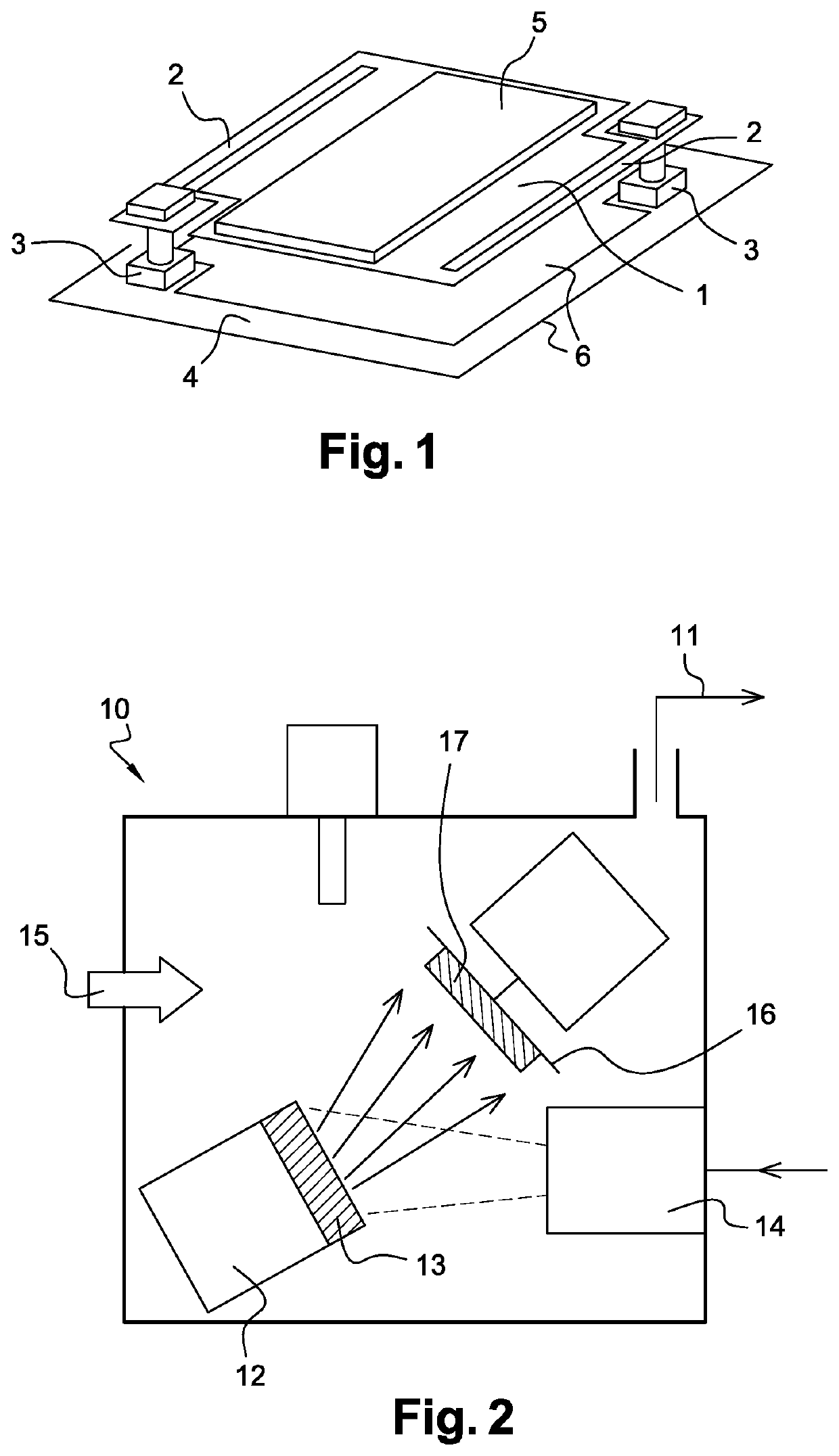
[0077]An elementary bolometric detector has been shown in FIG. 1. Such a detector is basically formed of a membrane (1) suspended via thermal insulation “arms” (2) and pillars (3), ensuring the electric connection with the substrate (4).

[0078]The membrane (1) comprises a thin film of thermistor material (5) on the most part of its surface, oriented opposite a window transparent to infrared radiation (and typically made of silicon or of germanium).

[0079]Advantageously, and to optimize the performance of the elementary detector, a metallic reflector film (6) is affixed under the suspended membrane and at an adequate distance therefrom, to form a resonating cavity and thus optimize the absorption of the infrared radiation.

[0080]The thermistor material (5) is made of a thin film of vanadium oxide VOx, having a typically thickness in the range from 20 to 200 nanometers and having a resistivity in the range from 6 ohm·cm to 50 ohm·cm. These resistivity values typically correspond to a val...


PUM

PropertyMeasurementUnit
temperatureaaaaaaaaaa
resistivityaaaaaaaaaa
temperatureaaaaaaaaaa

Abstract

An infrared radiation detector includes an array of elementary imaging bolometric detectors, each of the elementary bolometric detectors being formed of a bolometric membrane including a film made of vanadium oxide VOx, having a resistivity in the range from 6 ohm·cm to 50 ohm·cm, said membrane being suspended above a substrate integrating a signal for reading out the signal generated by said elementary detectors and for sequentially addressing the elementary detectors. The detector includes at least one getter intended to ensure the trapping of residual gas during and after the forming of the detector, and includes a hermetically-sealed cavity having said array and said at least one getter housed therein, having an upper cap including a window transparent to infrared radiation, said cap being sealed by means of a seal on a chip supporting the array of elementary detectors or on a package at the bottom of which the chip supporting the array of elementary detectors has been attached, said cavity being under vacuum or a low pressure.

Description

TECHNOLOGICAL FIELD[0001]The present disclosure relates to infrared imaging. More particularly, the present disclosure relates to the manufacturing of detectors of electromagnetic radiation, and particularly infrared radiation, integrating bolometric detectors.BACKGROUND[0002]In the field of infrared detectors, it is known to use devices arranged in an array and capable of operating at ambient temperature, that is, requiring no cooling at very low temperature, conversely to imaging devices called “quantum detectors”, which require an operation at very low temperature, typically that of liquid nitrogen.[0003]Such uncooled detectors conventionally use the variation of a physical quantity of an appropriate material, according to temperature, in the vicinity of 300 K. In the case of bolometric detectors, the physical quantity is electric resistivity.[0004]Such an uncooled detector generally associates:[0005]means for absorbing the infrared radiation and for converting it into heat,[0006...

Claims


Application Information

Patent Timeline
Patent Type & Authority Patents(United States)
IPC IPC(8): G01J5/20G01J5/04G01N21/3504
CPCG01J5/045G01J5/20G01N21/3504
Inventor CORTIAL, SÉBASTIENGUILLAUMONT, MARCPELENC, DENISZUCCHI, XAVIER
Owner COMMISSARIAT A LENERGIE ATOMIQUE ET AUX ENERGIES ALTERNATIVES
Why Eureka
Try Eureka