Semiconductor device
a technology of electromagnetic field and semiconductor, applied in galvano-magnetic devices, instruments, magnetic field offset compensation, etc., can solve the problems of increasing the amount of heat generated by excitation wiring, affecting the generation efficiency of calibration magnetic field, and prone to large variation in sensitivity and offset voltage characteristics. , to achieve the effect of suppressing intensity variation and characteristic fluctuation, enhancing the generation and increasing the efficiency of calibration magnetic field
- Summary
- Abstract
- Description
- Claims
- Application Information
AI Technical Summary
Benefits of technology
Problems solved by technology
Method used
Image
Examples
first embodiment
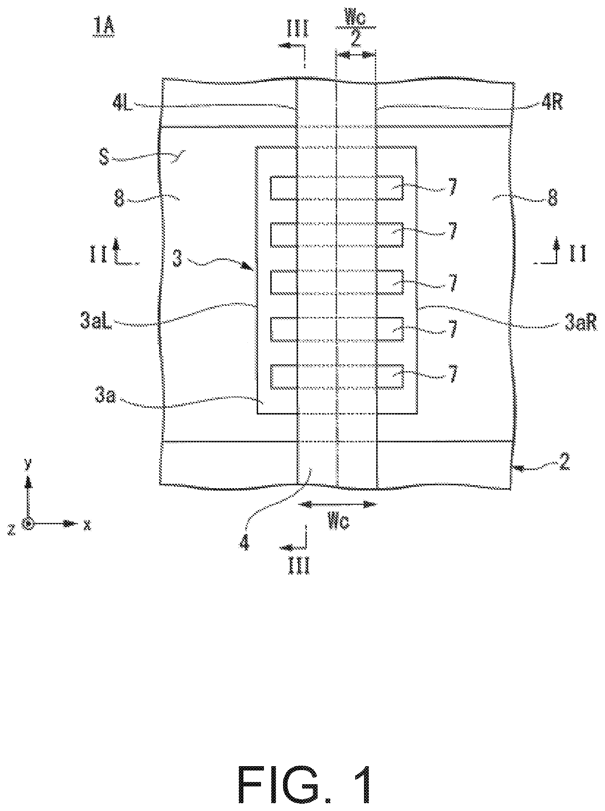
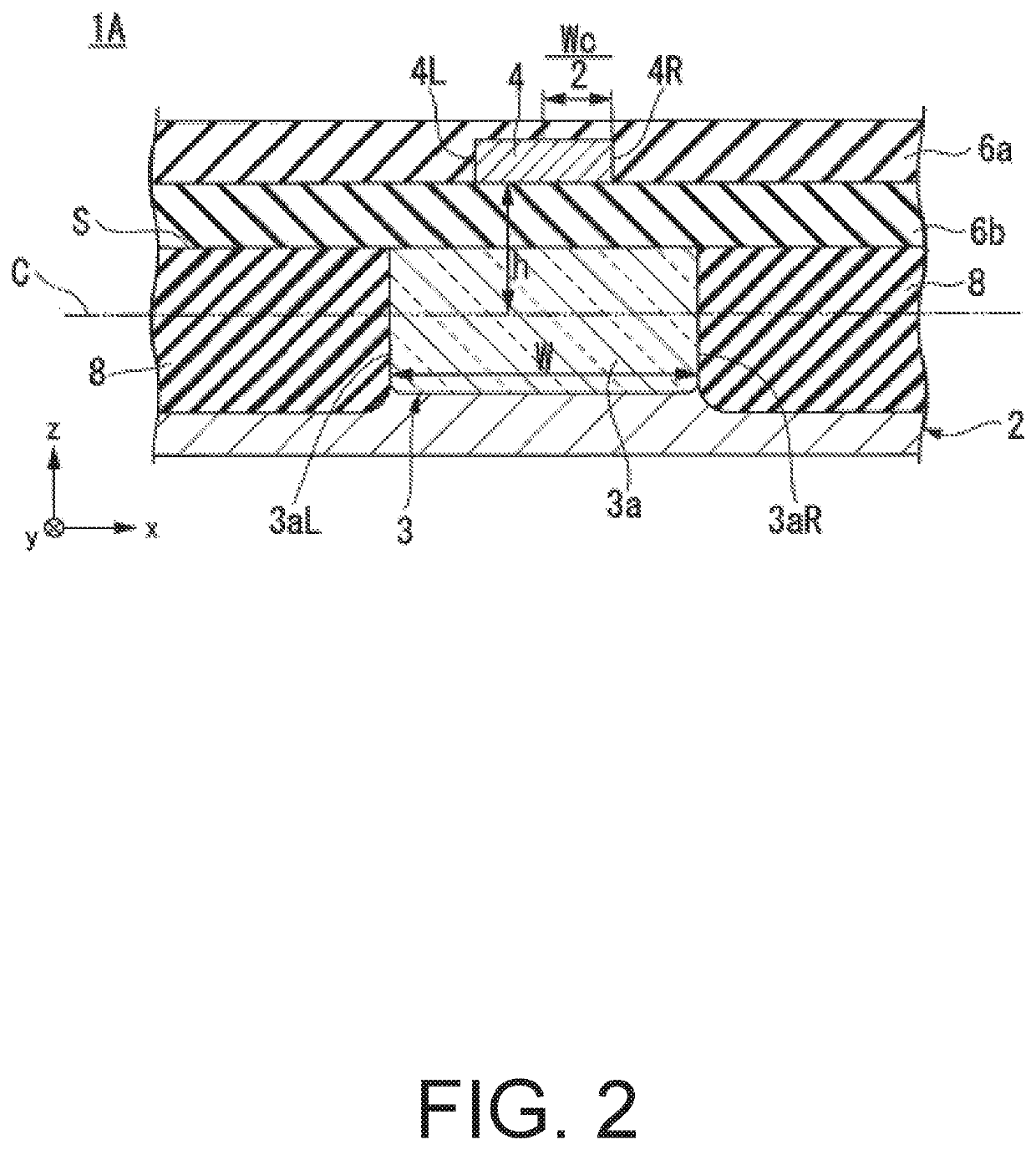
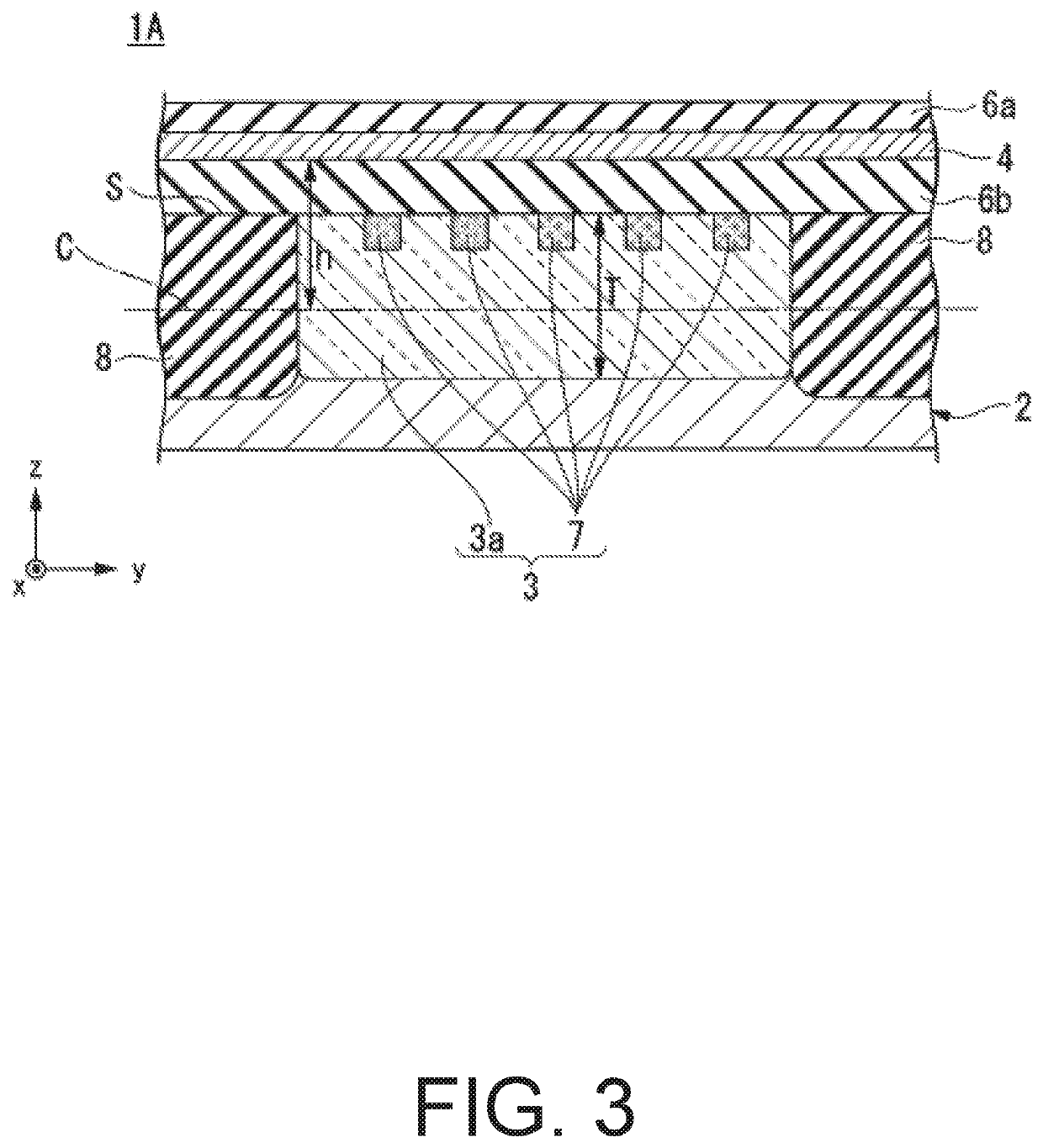
[0027]FIG. 1 is a plan view for illustrating a configuration of a semiconductor device 1A according to the first embodiment of the present invention. FIG. 2 is a sectional view of the semiconductor device 1A taken along the line II-II of FIG. 1 (II-II sectional view). FIG. 3 is a sectional view of a main part of the semiconductor device 1A taken along the line III-III of FIG. 1 (III-III sectional view of the main part). In FIG. 1, insulating layers 6a and 6b which appear in FIGS. 2 and 3 are omitted for ease of description.
[0028]As illustrated in FIG. 1, FIG. 2, and FIG. 3, the semiconductor device 1A includes a semiconductor substrate 2, a vertical Hall element 3 which includes a magnetosensitive portion 3a and is formed in the semiconductor substrate 2, and an excitation wiring 4 provided above the magnetosensitive portion 3a.
[0029]The semiconductor substrate 2 has the first conductivity type (for example, P type) which is one of a P type and an N type. Further, the semiconductor...
second embodiment
[0078]FIG. 7 is a plan view for illustrating a configuration of a semiconductor device 1B according to the second embodiment of the present invention. FIG. 8 is a sectional view of the semiconductor device 1B taken along the line VIII-VIII of FIG. 7 (VIII-VIII sectional view). In FIG. 7, insulating layers 6a and 6b are omitted for ease of description.
[0079]The semiconductor device 1B differs from the semiconductor device 1A because the excitation wiring 24 is provided in place of the excitation wiring 4, but other configurations are not substantially different therefrom. In the following description, equivalent components to those of the semiconductor device 1A are denoted by identical reference symbols, and duplicate descriptions thereof are omitted.
[0080]Similar to the excitation wiring 4, the excitation wiring 24 has an end surface 24R as the first end surface and an end surface 24L as the second end surface in a width direction and extends along a length direction. The excitatio...
PUM
| Property | Measurement | Unit |
|---|---|---|
| width | aaaaa | aaaaa |
| width | aaaaa | aaaaa |
| width | aaaaa | aaaaa |
Abstract
Description
Claims
Application Information
 - R&D
- Intellectual Property
- Life Sciences
- Materials
- Tech Scout
- Unparalleled Data Quality
- Higher Quality Content
- 60% Fewer Hallucinations
Browse by: Latest US Patents, China's latest patents, Technical Efficacy Thesaurus, Application Domain, Technology Topic, Popular Technical Reports.
© 2025 PatSnap. All rights reserved.Legal|Privacy policy|Modern Slavery Act Transparency Statement|Sitemap|About US| Contact US: help@patsnap.com


