Alloy nanomaterial, preparation method therefor, and semiconductor device

a nanomaterial and alloy technology, applied in the field of display material technology, can solve the problems of limiting the development and application of qd light-emitting display technologies, affecting the plurality of corresponding display technologies, and consuming a lot of research tim

Active Publication Date: 2022-08-02
TCL CORPORATION
View PDF9 Cites 2 Cited by
  • Summary
  • Abstract
  • Description
  • Claims
  • Application Information

AI Technical Summary

Benefits of technology

[0014]In view of the above problems in the existing technology, the objective of the present invention is to provide a quantum dot alloy nanomaterial, a preparation method, and a semiconductor device to improve the light-emitting performance of the existing QD materials, and thus solve the problem that the existing QD materials cannot meet the requirements of semiconductor devices.

Problems solved by technology

Although in recent years, the performance of QLED devices in all aspects has been continuously improved, there is still a considerable gap between the requirements of industrial applications and the basic device performance parameters, such as device efficiency, device stability, which also greatly hinders the development and application of the QD light-emitting display technologies.
Although QDs have been researched and developed as a classic nanomaterial for more than 30 years, a research time on using an excellent light-emitting properties of the QDs and using them as light-emitting materials in the QLED devices and a plurality of corresponding display technologies is still pretty short.
However, the QLED devices and a plurality of corresponding display technologies may be a complex photoelectronic device system, the performance of the device may be affected by many factors.
Even just considering the QD materials acting as the core light-emitting layer material, a plurality of QD performance metrics that need to be weighed are still much more complicated.
Totally, a traditional structure design for the QD considering only the improvement of the light-emitting properties of the QDs is impossible to meet the comprehensive requirements and the corresponding display technologies in a plurality of aspects including optical properties, electrical properties, processing properties and more of QD materials.
Due to the high surface atomic ratio of QD, atoms that do not form dangling bonds with surface ligands may exist as surface defect states, which may cause transitions through a non-radiative manner, so that greatly lowering the quantum yield of QDs.

Method used


Image

  • Alloy nanomaterial, preparation method therefor, and semiconductor device
  • Alloy nanomaterial, preparation method therefor, and semiconductor device
  • Alloy nanomaterial, preparation method therefor, and semiconductor device

Examples


example 1

on of CdZnSeS / CdZnSeS QDs

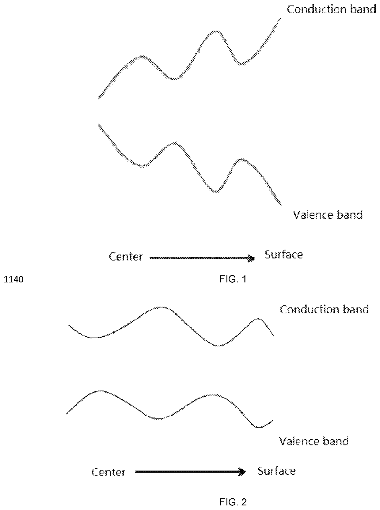
[0101]First, a cationic cadmium precursor, a cation zinc precursor, an anionic selenium precursor, and an anionic sulfur precursor may be injected into a reaction system to form a CdyZn1-ySebS1-b film (where 0≤y≤1, 0≤b≤1); continuously injecting the cationic cadmium precursor, the cationic zinc precursor, the anionic selenium precursor, and the anionic sulfur precursor into the reaction system to form a CdzZn1-zSeCS1-c film on a surface of the CdyZn1-ySebS1-b film. (where 0≤z≤1, and z is not equal to y, 0≤c≤1); under a plurality of reaction conditions including a certain heating temperature and heating time, Cd cations and Zn cations exchanges happen in the inner and the outer nanocrystals (that is, the two films of compounds described above); since the migration distance of the cation is limited and the migration probability decreases as the migration distance increases, thus a gradient alloy composition distribution with Cd and Zn concentrations, that is, ...

example 2

on of CdZnS / CdZnS QDs

[0102]First, a cationic cadmium precursor, a cationic zinc precursor, and an anionic sulfur precursor may be injected into a reaction system to form a CdyZn1-yS film (where 0≤y≤1); continuously injecting the cationic cadmium precursor, the cationic zinc precursor and the S precursor into the reaction system to form a CdzZn1-zS film on a surface of the CdyZn1-yS film. (where 0≤z≤1, and z is not equal to y); under a plurality of reaction conditions including a certain heating temperature and heating time, Cd cations and Zn cations exchanges happen in the inner and the outer nanocrystals (that is, the two films of compounds described above); since the migration distance of the cation is limited and the migration probability decreases as the migration distance increases, thus a gradient alloy composition distribution with Cd and Zn concentrations, that is, a CdxZn1-xS, where 0≤x≤1, is formed at an interface between the CdyZn1-yS film and the CdzZn1-zS film.

example 3

on of CdZnSe / CdZnSe QDs

[0103]First, a cationic cadmium precursor, a cationic zinc precursor, and an anionic Se precursor may be injected into a reaction system to form a CdyZn1-ySe film (where 0≤y≤1); continuously injecting the cationic cadmium precursor, the cationic zinc precursor, and the anionic Se precursor into the reaction system to form a CdzZn1-zSe film on a surface of the CdyZn1-ySe film. (where 0≤z≤1, and z is not equal to y); under a plurality of reaction conditions including a certain heating temperature and heating time, exchanges between the Cd cations and the Zn cations happen in the inner and the outer nanocrystals; since the migration distance of the cation is limited and the migration probability decreases as the migration distance increases, thus a gradient alloy composition distribution with Cd and Zn concentrations, that is, a CdxZn1-xSe, where 0≤x≤1, is formed at the interface between the CdyZn1-ySe film and the CdzZn1-zSe film.


PUM

PropertyMeasurementUnit
light-emission peak wavelengthaaaaaaaaaa
full width at half maximumaaaaaaaaaa
temperatureaaaaaaaaaa

Abstract

A quantum dot alloy nanomaterial, a preparation method therefor, and a semiconductor device. The quantum dot alloy nanomaterial comprises N alloy nanostructured units arranged in sequence in a radial direction, wherein N is larger than or equal to 2. The alloy nanostructured units comprise type A1 and type A2. Type A1 or type A2 is a gradient alloy component structure in which energy level width increases or decreases from inside out in the radial direction, respectively. In quantum dot alloy nanomaterial, alloy nanostructured units of type A1 and type A2 are alternately distributed, and the energy levels of adjacent alloy nanostructured units are continuous. The quantum dot alloy nanomaterial not only achieves higher luminous efficiency, but satisfies comprehensive performance requirements of a QLED device and a corresponding display technology for quantum dot alloy nanomaterial, and is an ideal material applicable to QLED and display technology.

Description

CROSS-REFERENCES TO RELATED APPLICATIONS[0001]This application is a national stage application of PCT Patent Application No. PCT / CN2017 / 080622, filed on 14 Apr. 2017, which claims priority to Chinese Patent Application No. 201611257332.3, filed on 30 Dec. 2016, the content of all of which is incorporated herein by reference.TECHNICAL FIELD[0002]The present invention relates to the field of a display material technology and, more particularly, relates to a quantum dot alloy nanomaterial, a preparation method, and a semiconductor device.BACKGROUND[0003]Quantum dot (QD) is a special material that is confined to a size in the order of nanometers in all three dimensions, The remarkable quantum confinement effect leads to many unique nano-properties of QDs, such as continuously-adjustable emission wavelength, narrow emission wavelength, wide absorption spectrum, high emission intensity, long fluorescence lifetime, excellent biocompatibility, etc. These features make the QDs own a wide ran...

Claims


Application Information

Patent Timeline
Patent Type & Authority Patents(United States)
IPC IPC(8): C09K11/88C09K11/56H01L51/50B82Y20/00B82Y40/00
CPCC09K11/883C09K11/565H01L51/502B82Y20/00B82Y40/00B82Y30/00H10K50/115H10K2102/00H01L33/18H01L33/28
Inventor YANG, YIXINGLIU, ZHENGQIAN, LEI
Owner TCL CORPORATION
Why Eureka
Try Eureka