Semiconductor device

a technology of semiconductor devices and dielectric films, applied in semiconductor devices, semiconductor/solid-state device details, electrical apparatus, etc., can solve the problems of reduced moisture resistance of semiconductor devices, and easy damage of conductors or insulating films directly below the pads, so as to reduce stress occurring in the dielectric films, suppress corrosion of conductors or other elements covered with dielectric films, and improve the film quality of dielectric films in the vicinity of bent sections

Active Publication Date: 2022-08-02
MURATA MFG CO LTD
View PDF15 Cites 0 Cited by
  • Summary
  • Abstract
  • Description
  • Claims
  • Application Information

AI Technical Summary

Benefits of technology

[0009]Accordingly, the present disclosure provides a semiconductor device capable of suppressing a reduction in the moisture resistance, the occurrence of cracks, or the like when it includes a structure in which a conductor is bent directly below a pad.
[0011]The film quality of the dielectric film in the vicinity of the bent section is improved, and moisture does not easily enter the dielectric film. Thus, corrosion of the conductor or other element covered with the dielectric film can be suppressed. Moreover, stress occurring in the dielectric film can be reduced. Thus, the occurrence of cracks or the like can be suppressed, and the reliability can be enhanced.

Problems solved by technology

Through that opening, unfortunately, moisture can easily enter the semiconductor device.
If the moisture through that opening reaches the conductor or other similar element directly below the bonding pad, corrosion of the conductor or other similar element advances, and the moisture resistance of the semiconductor device reduces.
In addition, for the POE structure, the conductor or an insulating film directly below the pad is susceptible to and easily damaged by an impact load during wire bonding.
With the inclusion of the slit, a supersonic energy applied to the protrusion electrode during wire bonding can easily dissipate.
For the semiconductor device disclosed in Japanese Unexamined Patent Application Publication No. 2007-67332, it is impossible to arrange the bent area in the conductor directly below the pad.

Method used


Image

  • Semiconductor device
  • Semiconductor device
  • Semiconductor device

Examples


first embodiment

[0026]A semiconductor device according to a first embodiment is described with reference to FIGS. 1A to 10.

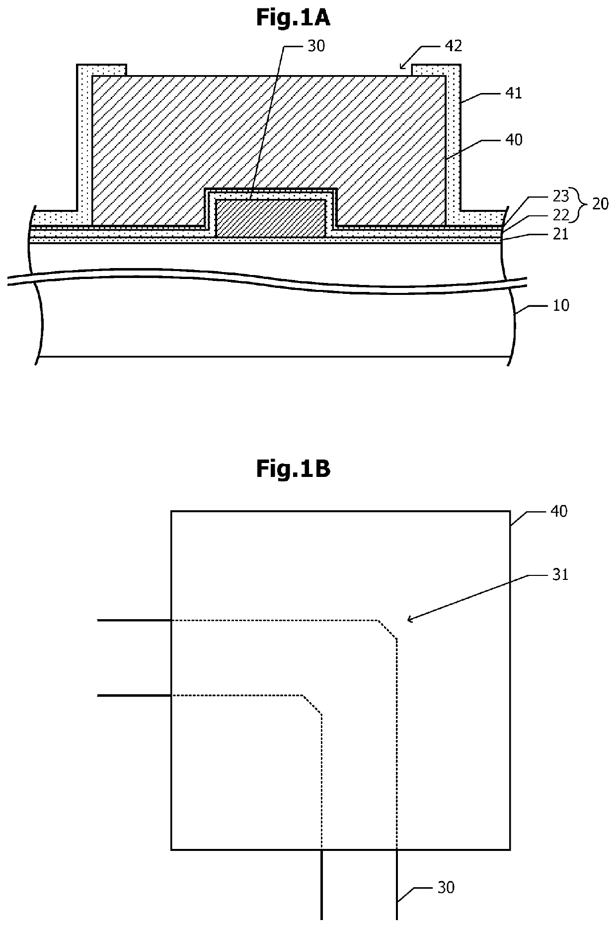
[0027]FIGS. 1A and 1B are a cross-sectional view and a plan view, respectively, of a portion of the semiconductor device according to the first embodiment. A first dielectric film 21 and a dielectric film 20 are disposed above a semiconductor substrate 10 in this order from the side of the semiconductor substrate 10. The dielectric film 20 includes two layers of a second dielectric film 22 and a third dielectric film 23. A conductor 30 is arranged on the first dielectric film 21. The conductor 30 is covered with the second dielectric film 22 and third dielectric film 23. That is, the conductor 30 is arranged between the semiconductor substrate 10 and dielectric film 20.

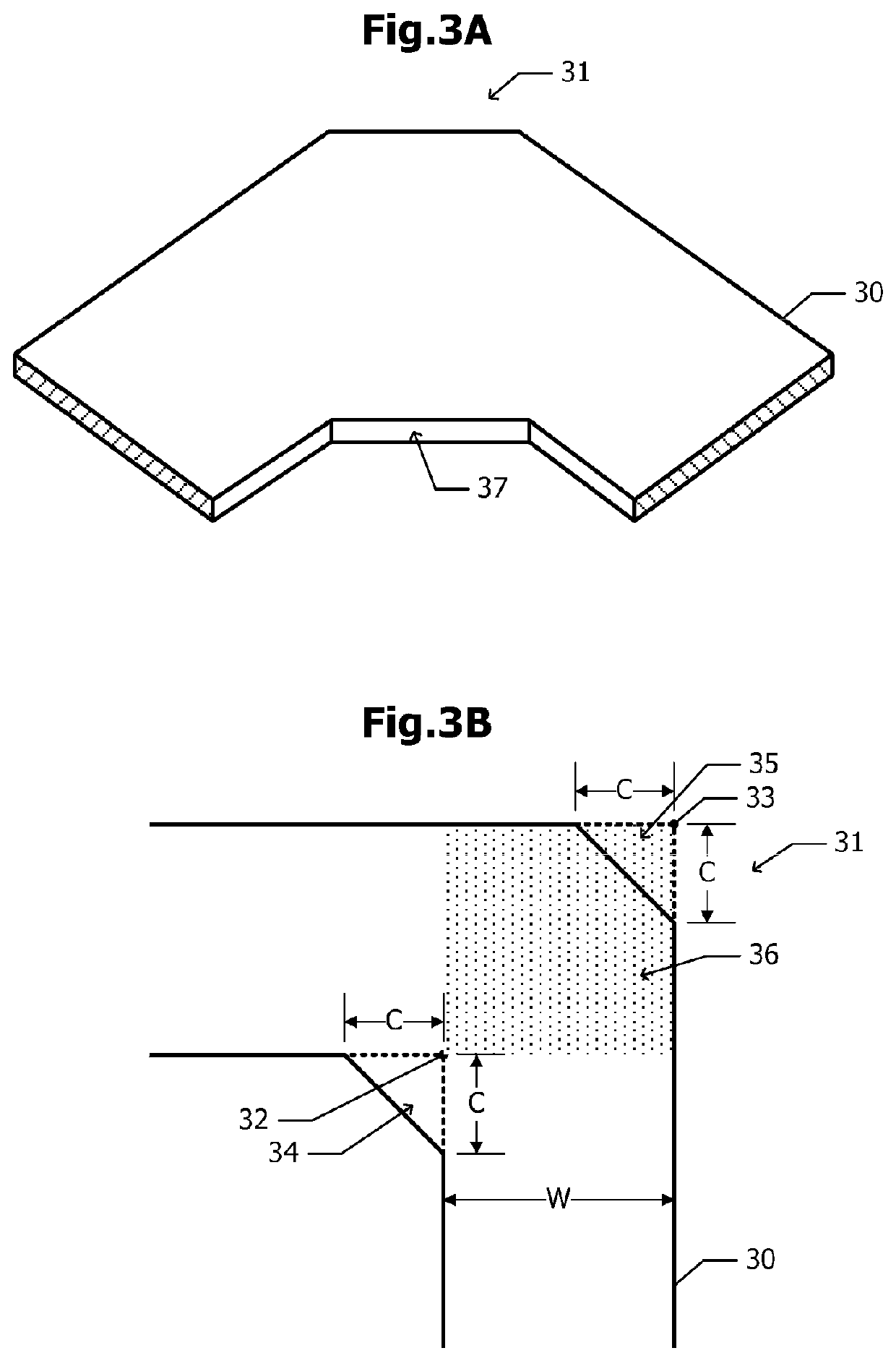
[0028]The conductor 30 is bent at a right angle at a bent section 31. A pad 40 is arranged on the dielectric film 20. The pad 40 overlaps the bent section 31 in the conductor 30 as seen in plan view. More specifi...

second embodiment

[0069]Next, a semiconductor device according to a second embodiment is described with reference to FIGS. 11A and 11B. The configuration common to the semiconductor device according to the first embodiment is not described here.

[0070]FIG. 11A is a perspective view of the conductors 30 in the semiconductor device according to the second embodiment. In the first embodiment, the inside and outside chamfered surfaces 37 (FIG. 3A) in the bent section 31 in each of the conductors 30 are plane. In the second embodiment, the chamfered surfaces 37 are round surfaces. That is, each of the chamfered surfaces 37 constitutes a portion of a cylindrical surface being in contact with the side surface of the straight-line segment of the conductor 30.

[0071]FIG. 11B illustrates graphs representing a result of simulation for stress occurring in the semiconductor device according to the second embodiment. The horizontal axis expresses the chamfer length C in the unit μm, and the vertical axis expresses t...

third embodiment

[0083]Next, a semiconductor device according to a third embodiment is described with reference to FIG. 13. The configuration common to the semiconductor device according to the first embodiment or second embodiment is not described here.

[0084]FIG. 13 is a plan view of the bent section 31 in the conductor 30 in the semiconductor device according to the third embodiment. In the first and second embodiments, the conductor 30 is bent at a right angle at the bent section 31 (FIGS. 3A, 3B, and other drawings). In the third embodiment, the bent angle θ of the conductor 30 at the bent section 31 is smaller than 90°. Thus, the segments of the conductor 30 on both sides of the bent section 31 meet at an obtuse angle.

[0085]In the case where the bent angle θ of the conductor 30 is smaller than 90°, when at least one of the outside corner and inside corner is chamfered, the stress occurring in the dielectric film 20 can be reduced.


PUM

PropertyMeasurementUnit
thicknessesaaaaaaaaaa

Abstract

A dielectric film is disposed on a semiconductor substrate, and a conductor including a bent section is arranged between the semiconductor substrate and the dielectric film. A pad is disposed on the dielectric film. The pad is covered with a protective film. The protective film has an opening through which an upper surface of the pad is exposed. The bent section in the conductor and the pad overlap each other as seen in plan view, and an inside corner and an outside corner in the bent section are chamfered.

Description

CROSS-REFERENCE TO RELATED APPLICATIONS[0001]This application claims benefit of priority to International Patent Application No. PCT / JP2018 / 025762, filed Jul. 6, 2018, and to Japanese Patent Application No. 2017-142972, filed Jul. 24, 2017, the entire contents of each are incorporated herein by reference.BACKGROUNDTechnical Field[0002]The present disclosure relates to a semiconductor device.Background Art[0003]To reduce the size of a chip, a pad-on-element (POE) structure, in which a conductor or other similar element is arranged directly below a bonding pad, is adopted. The bonding pad is overlaid with a protective film, and the protective film has an opening through which the upper surface of the bonding pad is exposed. Through that opening, unfortunately, moisture can easily enter the semiconductor device. If the moisture through that opening reaches the conductor or other similar element directly below the bonding pad, corrosion of the conductor or other similar element advances...

Claims


Application Information

Patent Timeline
Patent Type & Authority Patents(United States)
IPC IPC(8): H01L23/00H01L23/495
CPCH01L23/49555H01L24/05H01L24/13H01L24/45H01L2924/01079H01L2224/02166H01L2224/48463H01L23/5283H01L23/53295H01L23/3157H01L2224/0401H01L2224/04042H01L2224/13082H01L2224/05568H01L2224/05559H01L23/564H01L2224/05644H01L2224/13147H01L2224/131H01L2224/05166H01L24/48H01L2924/00014H01L2924/014
Inventor KUROKAWA, ATSUSHITOKUYA, HIROAKIKOBAYASHI, KAZUYASANO, YUICHI
Owner MURATA MFG CO LTD
Why Eureka
Try Eureka