Apparatus for collecting by-product of semiconductor manufacturing process

a technology of semiconductor manufacturing process and apparatus, which is applied in the direction of auxillary pretreatment, sustainable manufacturing/processing, and separation processes, etc., can solve the problems of increasing exhaust pressure, complicated internal structure of apparatus, and contamination of wafers in process chambers

Active Publication Date: 2022-10-04
MILAEBO
View PDF9 Cites 0 Cited by
  • Summary
  • Abstract
  • Description
  • Claims
  • Application Information

AI Technical Summary

Benefits of technology

[0020]Accordingly, the present invention has been made keeping in mind the above problems occurring in the related art, and an objective of the present invention is intended to provide an apparatus for collecting a by-product in a semiconductor manufacturing process, the apparatus including: a heating jacket provided detachably on a housing unit to provide a uniform temperature in the collecting space into which exhaust gas containing tungsten hexafluoride (WF6) discharged after being used in a semiconductor manufacturing process flows such that a collecting region is adjusted; and upper and lower internal collecting towers configured to realize sufficient moving path and time in a narrow collecting space to collect the by-product efficiently.
[0021]It is another objective of the present invention to provide an apparatus for collecting a by-product in a semiconductor manufacturing process, the apparatus having a housing unit configured to prevent an inner wall surface of a housing main body from being damaged when cleaning a space inside the housing unit by a sand blasting method after the by-product collecting process, and configured to be quickly replaceable when the cleaning is difficult.

Problems solved by technology

During the process, a large amount of various ignitable gases and hazardous gases containing corrosive foreign substances and toxic components are produced in the process chamber.
However, the scrubber only treats and removes a by-product which is in a form of gas.
Thus, when the by-product is discharged to the outside of the process chamber and then solidified, the by-product is adhered to an exhaust line, leading to increasing exhaust pressure.
In addition, the by-product is introduced into the vacuum pump and causes a failure of the vacuum pump and backflow of the hazardous gas, leading to contamination of the wafer in the process chamber.
However, the apparatus is designed to have a dedicated heating device, so that the internal structure thereof is complicated.
In addition, the conventional apparatus for collecting the exhaust gas containing tungsten hexafluoride (WF6) has a problem in structure in that the sufficient distance for gas movement cannot be secured in a state where the reaction space is narrow and limited and the high internal temperature is maintained such that tungsten hexafluoride (WF6) is sufficiently reacted and discharged without being captured.
In addition, due to the structural characteristic in which the heating device is provided inside the apparatus, the heating device is continuously exposed to the exhaust gas.
Therefore, the durability thereof is lowered due to corrosion or deterioration, and the repairing or replacement cycle is short so that the continuous operation is difficult and the maintenance cost is increased.
Thus, there is a problem in structure in terms of the cleaning process that, as the cleaning process is repeated, an inner wall of the housing of the apparatus is required to be replaced when damage occurs due to impact by sands sprayed at a high pressure.

Method used


Image

  • Apparatus for collecting by-product of semiconductor manufacturing process
  • Apparatus for collecting by-product of semiconductor manufacturing process
  • Apparatus for collecting by-product of semiconductor manufacturing process

Examples


Embodiment Construction

[0063]Hereinafter, specific structural and functional descriptions of embodiments of the present invention will be described in detail with reference to the accompanying drawings. In the following description, it is to be noted that, when the functions of conventional elements and the detailed description of elements related with the present invention may make the gist of the present invention unclear, a detailed description of those elements will be omitted.

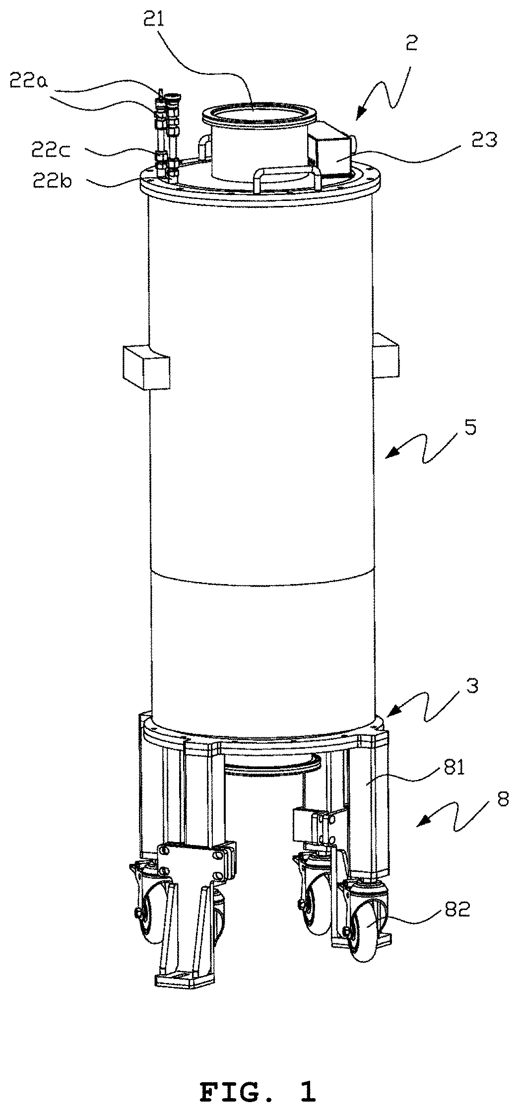
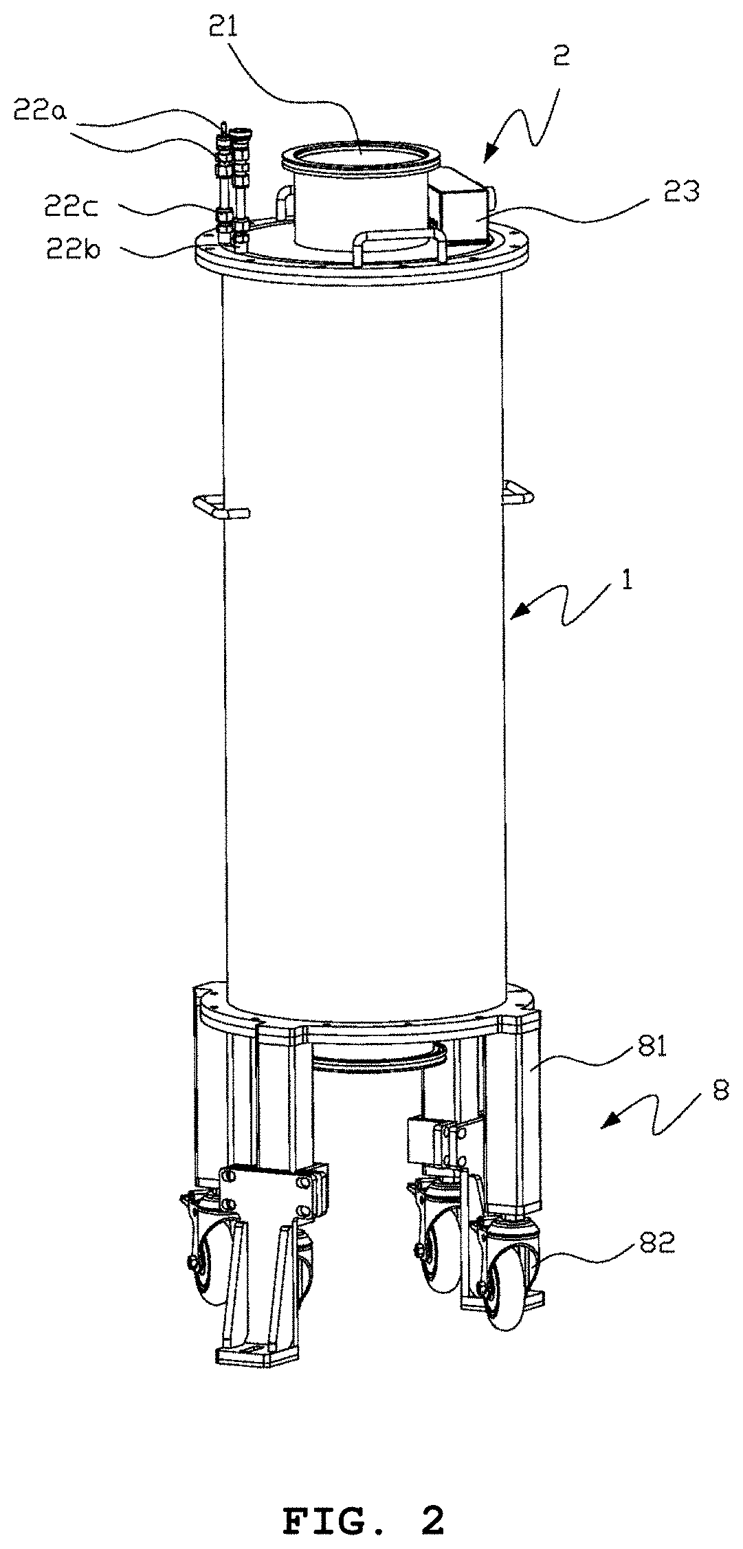
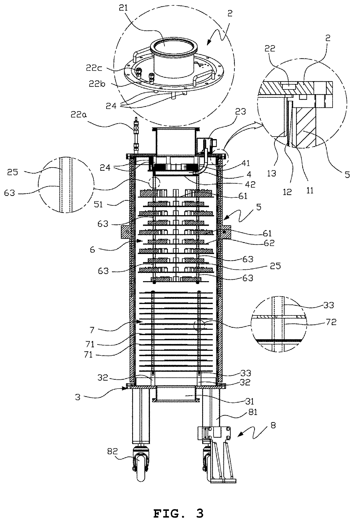
[0064]FIG. 1 is a perspective view of an apparatus for collecting a by-product according to an embodiment of the present invention; FIG. 2 is an exploded-perspective view of the apparatus for collecting a by-product in which a heating jacket is removed according to the embodiment of the present invention; FIG. 3 is a cross-sectional view of an internal structure of the apparatus for collecting a by-product according to the embodiment of the present invention; FIG. 4 is a view of a structure of a housing unit according to the emb...


PUM

PropertyMeasurementUnit
temperatureaaaaaaaaaa
outer circumferenceaaaaaaaaaa
distanceaaaaaaaaaa

Abstract

Disclosed is an apparatus for collecting a by-product in a semiconductor manufacturing process, the apparatus including: a heating jacket provided detachably along an outer circumference of a housing unit to provide a uniform temperature in a space into which exhaust gas containing tungsten hexafluoride (WF6) discharged after being used in a semiconductor manufacturing process flows; an upper internal collecting tower having first collecting plates and second collecting plates alternately arranged at regular intervals in a vertical direction to realize sufficient moving path and time in a narrow space; and a lower internal collection tower having third collecting plates arranged at regular intervals in the vertical direction, the third collecting plates having different regions on each surface thereof such that each of the third collecting plates is misaligned with a next third collecting plate to realize sufficient moving path and time in a narrow space.

Description

CROSS REFERENCE TO RELATED APPLICATION[0001]The present application claims priority to Korean Patent Application No. 10-2019-0038416, filed Apr. 2, 2019, the entire contents of which is incorporated herein for all purposes by this reference.BACKGROUND OF THE INVENTIONField of the Invention[0002]The present invention relates to an apparatus for collecting a by-product in a semiconductor manufacturing process. More particularly, the present invention relates to an apparatus for collecting a by-product, the apparatus being configured to maintain a reaction temperature therein uniformly at a high temperature to efficiently collect a by-product containing tungsten hexafluoride in exhaust gas components discharged to a scrubber after physical and chemical processes of depositing a thin film on a wafer in a process chamber and etching the wafer, and the apparatus being also configured to realize sufficient collection paths and to facilitate cleaning the apparatus.Description of the Related...

Claims


Application Information

Patent Timeline
Patent Type & Authority Patents(United States)
IPC IPC(8): H01L21/67C23C16/44B01D51/02
CPCH01L21/67017B01D51/02C23C16/4412B01D46/12B01D2258/0216B01D2257/204H01L21/67109C23C16/14B01D47/12Y02P70/50H01L21/67098B01D53/005
Inventor CHO, CHE HOOLEE, YEON JUKIM, JI SU
Owner MILAEBO
Why Eureka
Try Eureka