Circuit board having copper clad laminate laminated on core layer, and electronic device comprising same

a technology of circuit board and core layer, which is applied in the direction of circuit bendability/stretchability, substantially flat resonant elements, and resonant antennas, etc., can solve the problems of increased manufacturing cost and manufacturing time of products, increased signal loss, etc., to reduce signal loss in signal lines, reduce manufacturing time, and reduce signal loss

Active Publication Date: 2022-11-22
SAMSUNG ELECTRONICS CO LTD
View PDF15 Cites 0 Cited by
  • Summary
  • Abstract
  • Description
  • Claims
  • Application Information

AI Technical Summary

Benefits of technology

[0005]In a multilayer rigid-flexible circuit board, with reference to a flexible circuit board, a plurality of substrates including circuit layers and insulating layers may be disposed above the rigid circuit board through lamination and a plurality of substrates including relatively fewer circuit layers and insulating layers than the substrates disposed above the rigid circuit board may be disposed below the rigid circuit board through lamination. For example, seven substrate layers may be disposed above the rigid circuit board through a seven-step process, and five substrate layers may be disposed below the rigid circuit board through a five-step process. In this case, the substrate layers disposed above and below the rigid circuit board are unbalanced, and due to this, a signal loss may increase due to a change in impedance of high-speed wiring signal lines (e.g., signal lines and RF signal lines) in the multilayer rigid-flexible circuit board area. In addition, when the number of laminated substrate layers increases in the multilayer rigid-flexible circuit board, the manufacturing cost and manufacturing time of a product may increase.
[0006]An embodiment of the disclosure is capable of providing an electronic device including a circuit board, which enables a signal loss caused due to a change in impedance of high-speed wiring signal lines (e.g., signal lines or RF signal lines) in a circuit board area to be reduced by disposing substrate layers above and below the core layer of the circuit board in a balanced manner.
[0011]According to at least one of the above-described solutions to problems of the disclosure, with reference to a core layer on the circuit board according to an embodiment of the disclosure, by evenly disposing the first and second flexible copper clad laminates and at least one first and second substrate layer symmetrical to each other above and below the core layer, even when high-speed signal lines (e.g., signal lines and RF signal lines) are laid on the circuit board, it is possible to reduce a signal loss caused due to a change in impedance of the high-speed wiring signal lines in the circuit board area and to achieve signal integrity and stabilization of radio frequency interference (RFI). In other words, in the past, since seven substrate layers are disposed above the core layer and five substrate layers are disposed below the core layer, and thus substrate layers are unevenly disposed above and below the core layer, the signal loss increases in the signal lines and the RF signal lines of the circuit board and manufacturing steps and a manufacturing time increase. However, in the circuit board according to an embodiment of the disclosure, by evenly disposing substrate layers such that five substrate layers are disposed above the core layer and five substrate layers are disposed below the core layer, it is possible to reduce the signal loss in signal lines and RF signal lines of a product. Furthermore, due to the reduction of the number of laminated substrate layers, it is possible to reduce the manufacturing steps and time of the product, and it is also possible to reduce the manufacturing costs of the product.
[0012]According to an embodiment, with respect to the core layer of a circuit board between the first and second rigid circuit boards, by symmetrically disposing first and second flexible circuit boards above and below the core layer, it is possible to implement bending using the first and second flexible circuit boards between the first and second rigid circuit boards and to stably maintain the bent state. Similarly, it is also possible to reduce the signal loss caused due to a change in impedance in the high-speed wiring signal lines (e.g., a signal line and an RF signal line in the area of the first and second flexible circuit boards).

Problems solved by technology

In this case, the substrate layers disposed above and below the rigid circuit board are unbalanced, and due to this, a signal loss may increase due to a change in impedance of high-speed wiring signal lines (e.g., signal lines and RF signal lines) in the multilayer rigid-flexible circuit board area.
In addition, when the number of laminated substrate layers increases in the multilayer rigid-flexible circuit board, the manufacturing cost and manufacturing time of a product may increase.

Method used


Image

  • Circuit board having copper clad laminate laminated on core layer, and electronic device comprising same
  • Circuit board having copper clad laminate laminated on core layer, and electronic device comprising same
  • Circuit board having copper clad laminate laminated on core layer, and electronic device comprising same

Examples


Embodiment Construction

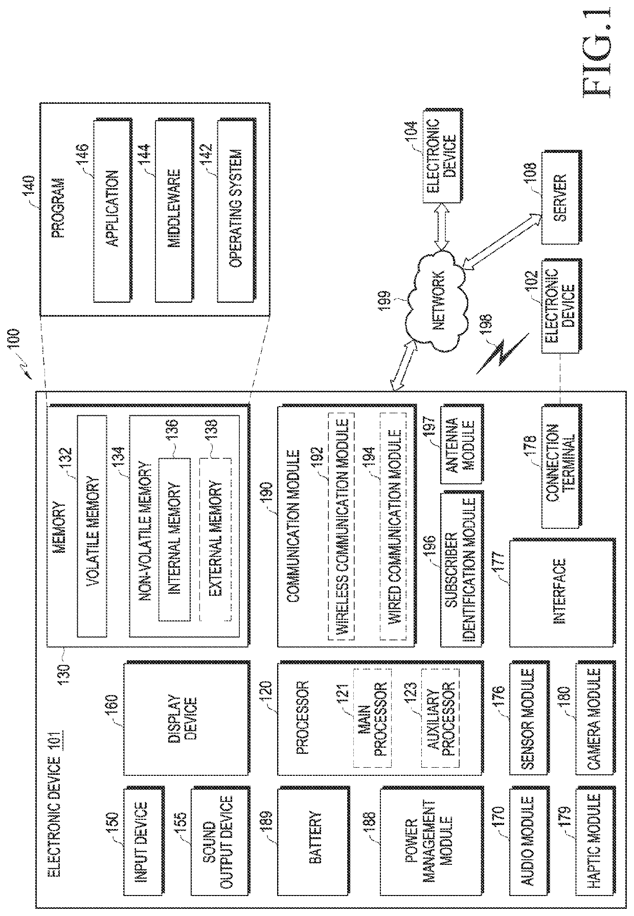
[0026]FIG. 1 is a block diagram illustrating an electronic device 101 in a network environment 100 according to various embodiments.

[0027]Referring to FIG. 1, the electronic device 101 in the network environment 100 may communicate with an electronic device 102 via a first network 198 (e.g., a short-range wireless communication network), or an electronic device 104 or a server 108 via a second network 199 (e.g., a long-range wireless communication network). According to an embodiment, the electronic device 101 may communicate with the electronic device 104 via the server 108. According to an embodiment, the electronic device 101 may include a processor 120, memory 130, an input device 150, a sound output device 155, a display device 160, an audio module 170, a sensor module 176, an interface 177, a haptic module 179, a camera module 180, a power management module 188, a battery 189, a communication module 190, a subscriber identification module (SIM) 196, or an antenna module 197. I...


PUM

PropertyMeasurementUnit
areasaaaaaaaaaa
frequencyaaaaaaaaaa
frequencyaaaaaaaaaa

Abstract

Disclosed are various embodiments related to a circuit board included in an electronic device. According to one embodiment, the circuit board may comprise: a core layer including an upper surface and a lower surface and formed as a substrate made of a prepreg material; a first flexible copper clad laminate including a plurality of conductive layers and laminated on the upper surface; at least one first substrate layer laminated above the first flexible copper clad laminate and including a conductive layer formed on the substrate made of a prepreg material; a second flexible copper clad laminate including a plurality of conductive layers and laminated on the lower surface; and at least one second substrate layer laminated under the second flexible copper clad laminate and including a conductive layer formed on the substrate made of a prepreg material. Various other embodiments are also possible.

Description

CROSS-REFERENCE TO RELATED APPLICATION(S)[0001]This application is a National Phase Entry of PCT International Application No. PCT / KR2019 / 009614, which was filed on Aug. 1, 2019, and claims priority to Korean Patent Application No. 10-2018-0091960, which was filed on Aug. 7, 2018 in the Korean Intellectual Property Office, the contents of each of which are incorporated herein by reference.BACKGROUND1. Field[0002]Various embodiments of the disclosure relate to a circuit board and an electronic device including the circuit board.2. Description of the Related Art[0003]Electronic devices may output information stored therein as sound or an image. As the degree of integration of electronic devices has increased and super-high-speed and large-capacity RF communication has become popular, multiple functions have recently come to be provided in a single electronic device, such as a mobile communication terminal. For example, various functions, such as an entertainment function (e.g., a game...

Claims


Application Information

Patent Timeline
Patent Type & Authority Patents(United States)
IPC IPC(8): H01Q1/38H05K1/02H01Q1/48H01Q9/04H05K1/09H05K1/11H05K1/14
CPCH05K1/0277H01Q1/48H01Q9/0407H05K1/0243H05K1/09H05K1/115H05K1/14H05K2201/04H05K2201/10098H05K3/4691H05K1/025
Inventor LEE, YOUNGSUNHONG, EUNSEOKKIM, BYEONGKEOLJEON, JONGMIN
Owner SAMSUNG ELECTRONICS CO LTD
Why Eureka
Try Eureka