

Compound semiconductor device
- Summary
- Abstract
- Description
- Claims
- Application Information
AI Technical Summary
Benefits of technology
Problems solved by technology
Method used
Image

Examples
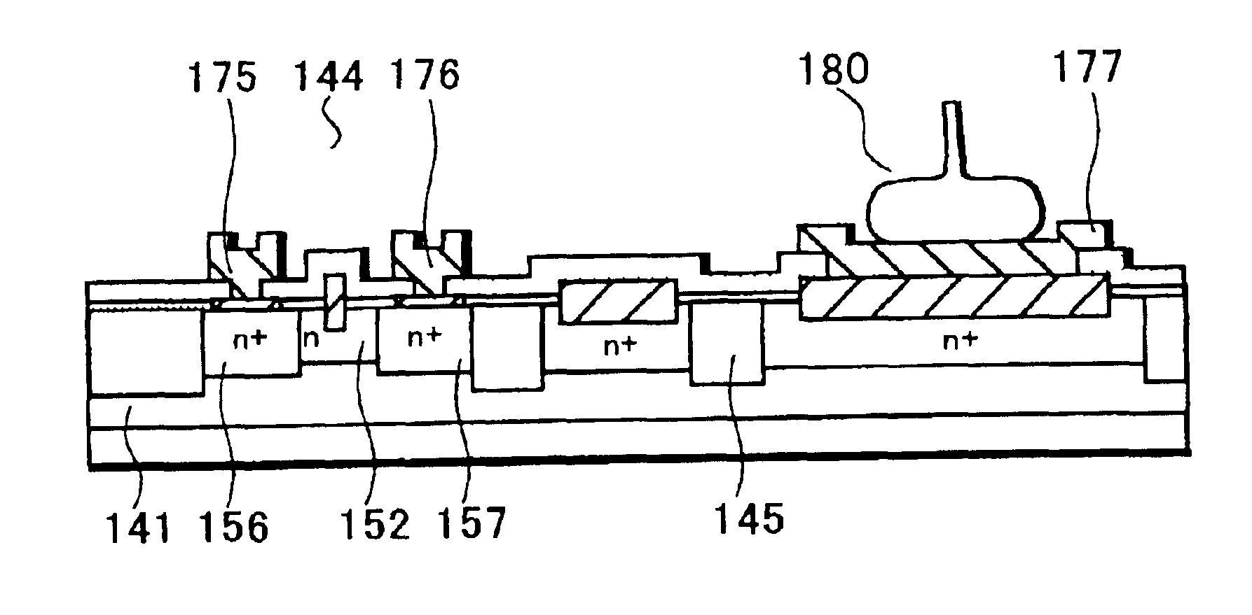
first embodiment
this invention will be described hereinafter in reference to FIG. 1 through FIG. 8.
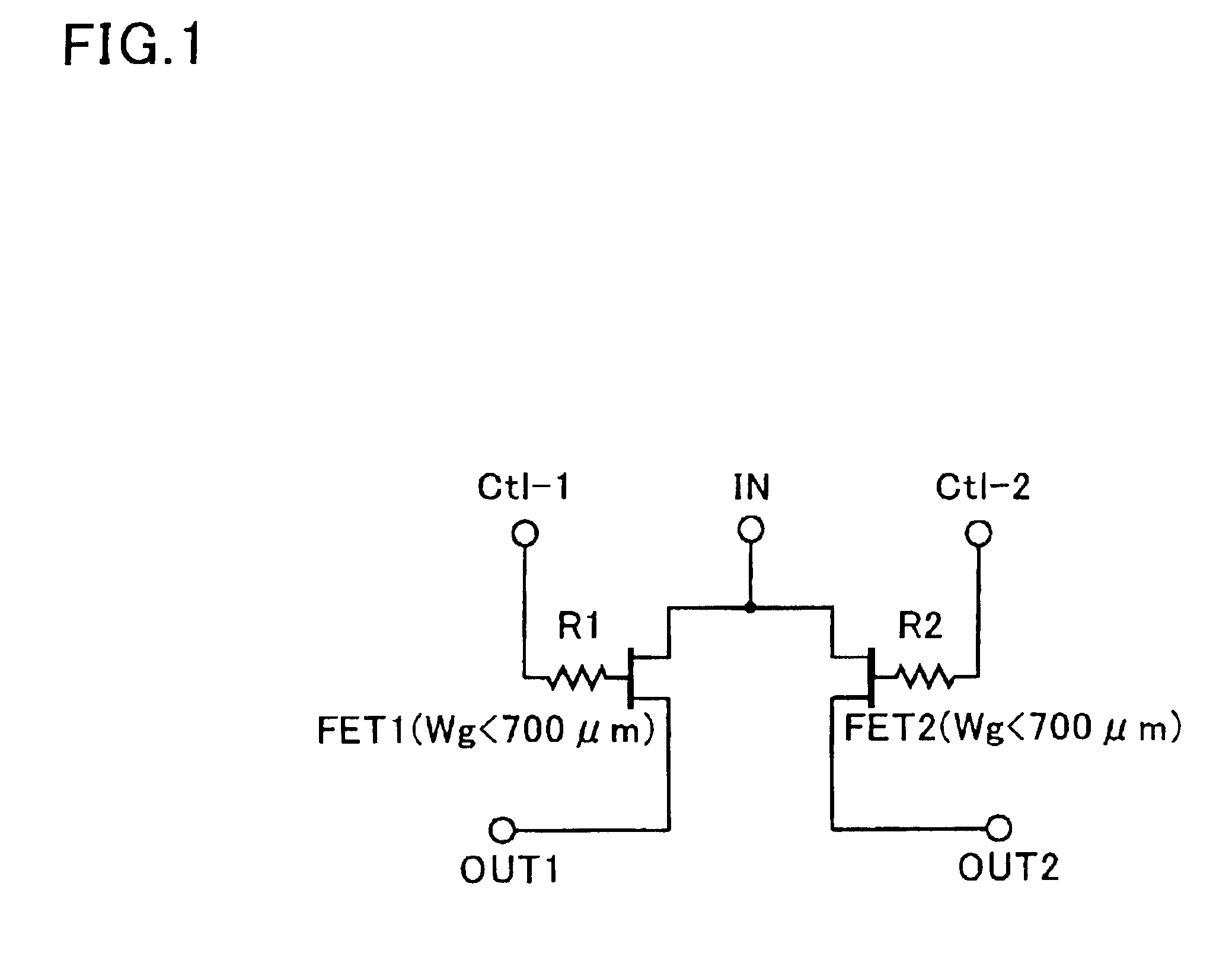
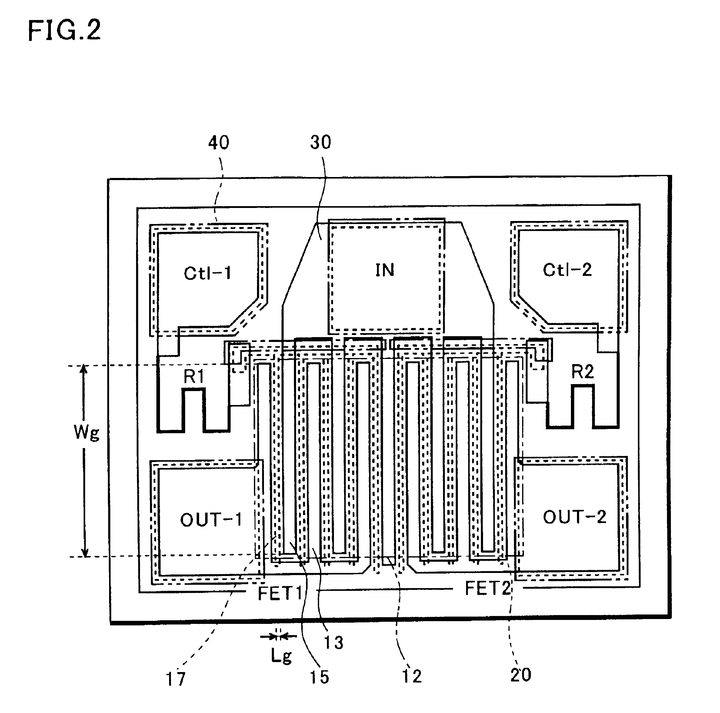
FIG. 1 is a circuit diagram for describing the compound semiconductor device of this invention. One of the two signal electrodes, which can be either a source electrode or a drain electrode, of each FET (FET1 denoting the first FET and FET2 denoting the second FET) is connected to a common electrode IN. Another of the two signal electrodes of each FET (FET1 and FET2) is connected to an output terminal (OUT1 and OUT2). The gate of FET1 and that of FET2 are connected to the control terminals Ctl-1 and Ctl-2 through resistors R1 and R2, respectively. A complementary signal is applied to the first and second control terminals Ctl-1 and Ctl-2. When a high level signal is applied to the control terminal of an FET of the two FETs, the FET changes to an on-state and forms a signal pass from the common input terminal IN to the output terminal of the FET (OUT1 or OUT2). The role of the resistors R1 and R2 is to...
PUM
 Abstract
Description
Claims
Application Information