Bus driver having noise removing circuit formed by pull-up resistor
- Summary
- Abstract
- Description
- Claims
- Application Information
AI Technical Summary
Problems solved by technology
Method used
Image

Examples
first embodiment
[0026] In FIG. 5, which illustrates the bus driver according to the present invention, the bus driver includes a MOS transistor 1 as a switching element having a gate connected to an input terminal IN for receiving an input voltage V.sub.in, a drain connected to an output terminal OUT for generating an output voltage V.sub.out, and a source connected to the ground terminal GND. Also, the bus driver includes a noise removing circuit formed by a pull-up resistor 2-1.
second embodiment
[0027] In FIG. 6, which illustrates the bus driver according to the present invention, the bus driver includes a bipolar transistor 1' instead of the MOS transistor 1 of FIG. 5. The bipolar transistor 1' has a base connected to the input terminal IN, a collector connected to the output terminal OUT, and an emitter connected to the ground terminal GND. The bus driver of FIG. 6 operates in the same way as the bus driver of FIG. 5.
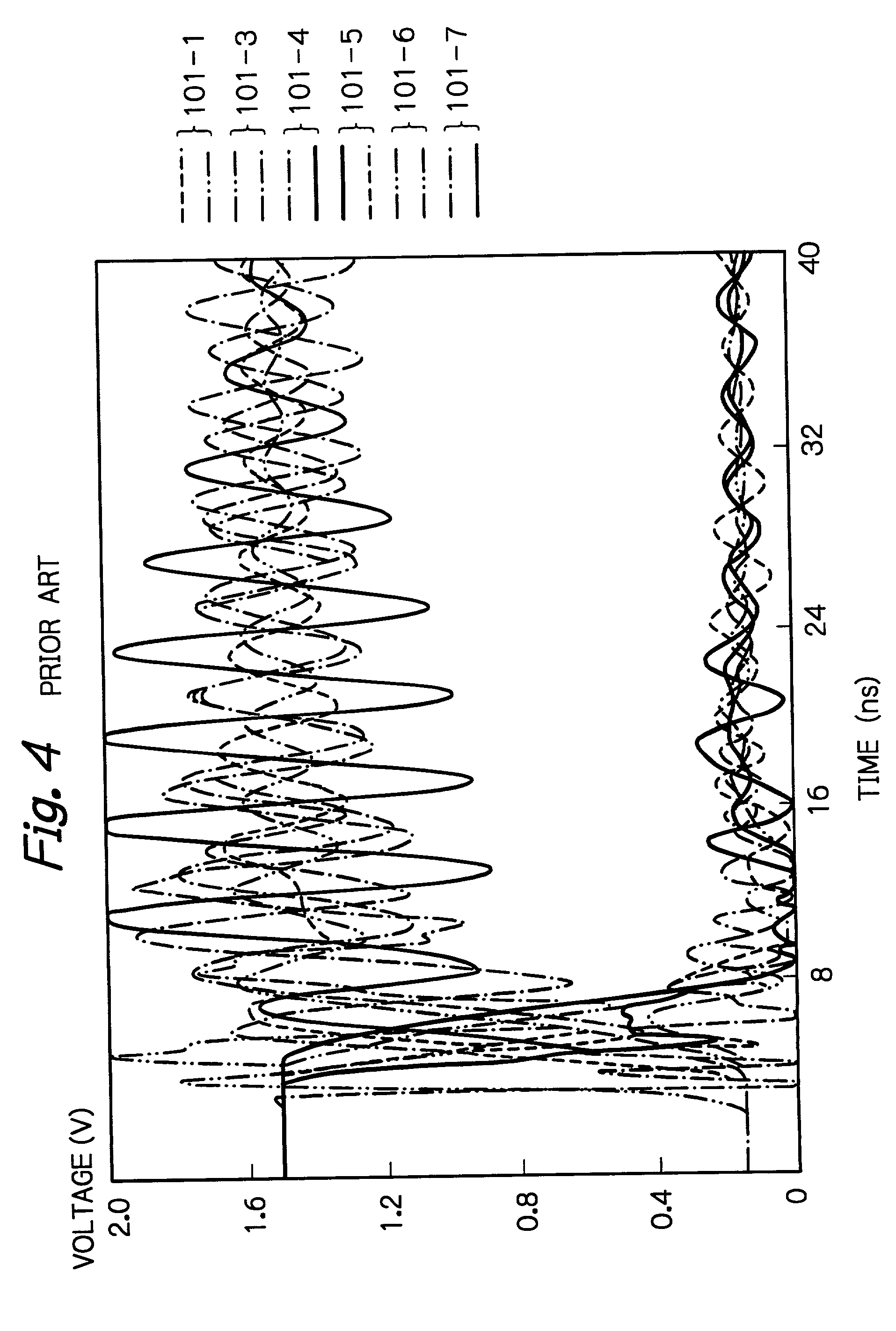
[0028] Assume that the bus driver of FIG. 5 or 6 is applied to the data processing system of FIGS. 1 and 3. In this case, when the input voltage V.sub.in, of the bus driver of FIG. 5 or 6 included in the package 101-3 is switched from high to low and vice versa, the voltages at the bus receivers at the packages 101-1, 101-3, 101-4, . . . , 101-7 are obtained as shown in FIG. 7. As shown in FIG. 7, the ringing effect generated in each of the voltages of the bus receivers is reduced, since the bus driver of FIG. 5 or 6 has a noise removing circuit formed by the...
third embodiment
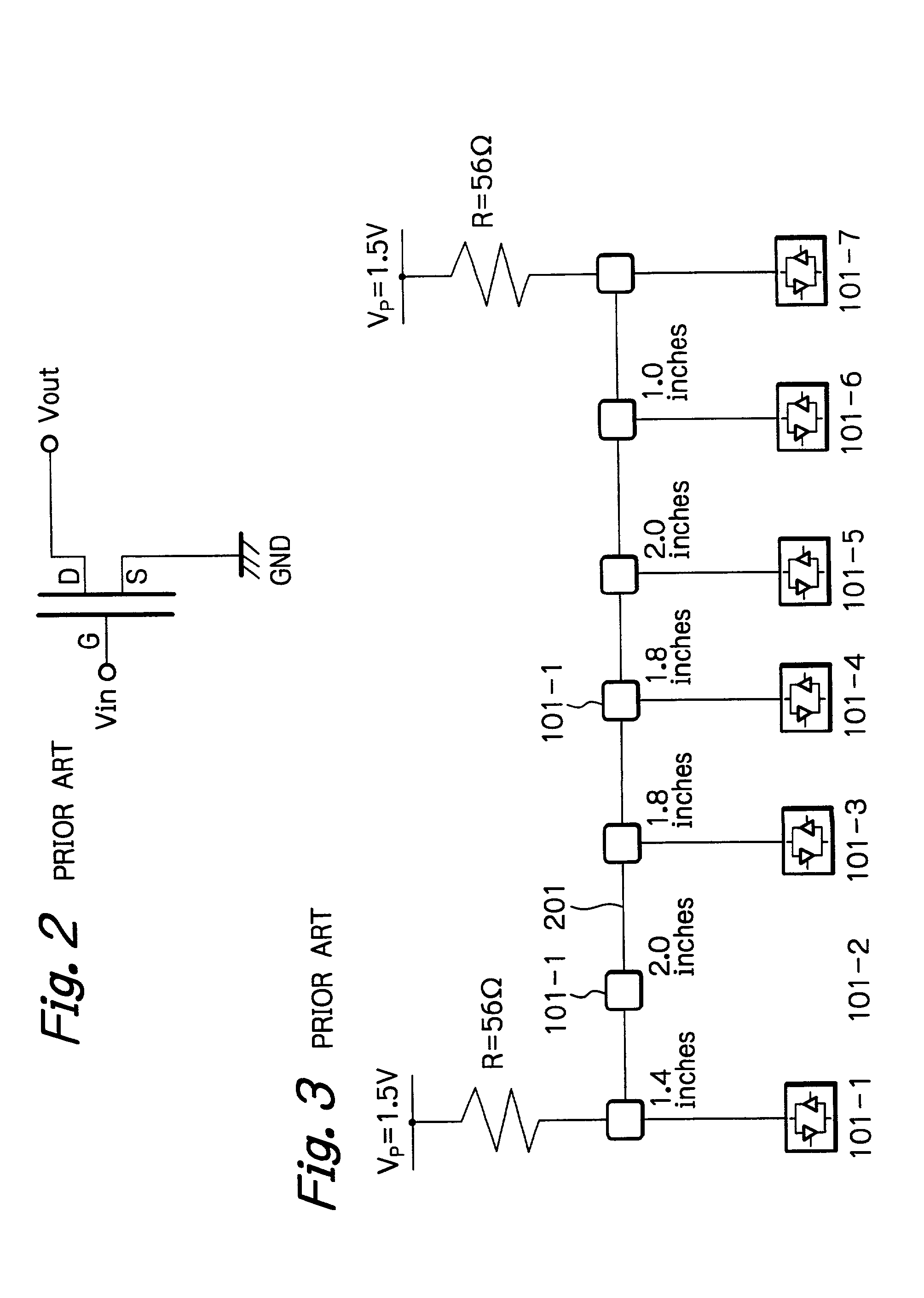
[0029] In FIG. 8, which illustrates the present invention, one pull-up resistor R' formed on the back panel 200 is connected to the connector 101-1 of each of the packages 101-2, 101-3, 101-4, 101-5 and 101-6 of FIG. 3. Note that each of the packages 101-1, 101-3, 101-4, 101-5, 101-6 and 101-7 includes an open drain type MOS transistor as a bus driver or a bus receiver as illustrated in FIG. 2; however, this bus driver or bus receiver can be an open collector type bipolar transistor as illustrated in FIG. 9.
[0030] In FIG. 8, when the input voltage V.sub.in, of the bus driver included in the package 101-3 is switched from high to low and vice versa, the voltages at the bus receivers at the packages 101-1, 101-3, 101-4, . . . , 101-7 are obtained in a similar way to that of FIG. 7. That is , the ringing effect generated in each of the voltages of the bus receivers is reduced, since packages 101-2, 101-3, 101-4 101-5, 101-6 has a noise removing circuit formed by the pull-up resistor R'...
PUM
 Abstract
Description
Claims
Application Information