

Electronic device
a display device and electronic technology, applied in the field of electronic devices, can solve the problems of deterioration of tfts, not large deterioration of tfts,
- Summary
- Abstract
- Description
- Claims
- Application Information
AI Technical Summary
Benefits of technology
Problems solved by technology
Method used
Image

Examples
embodiment 2
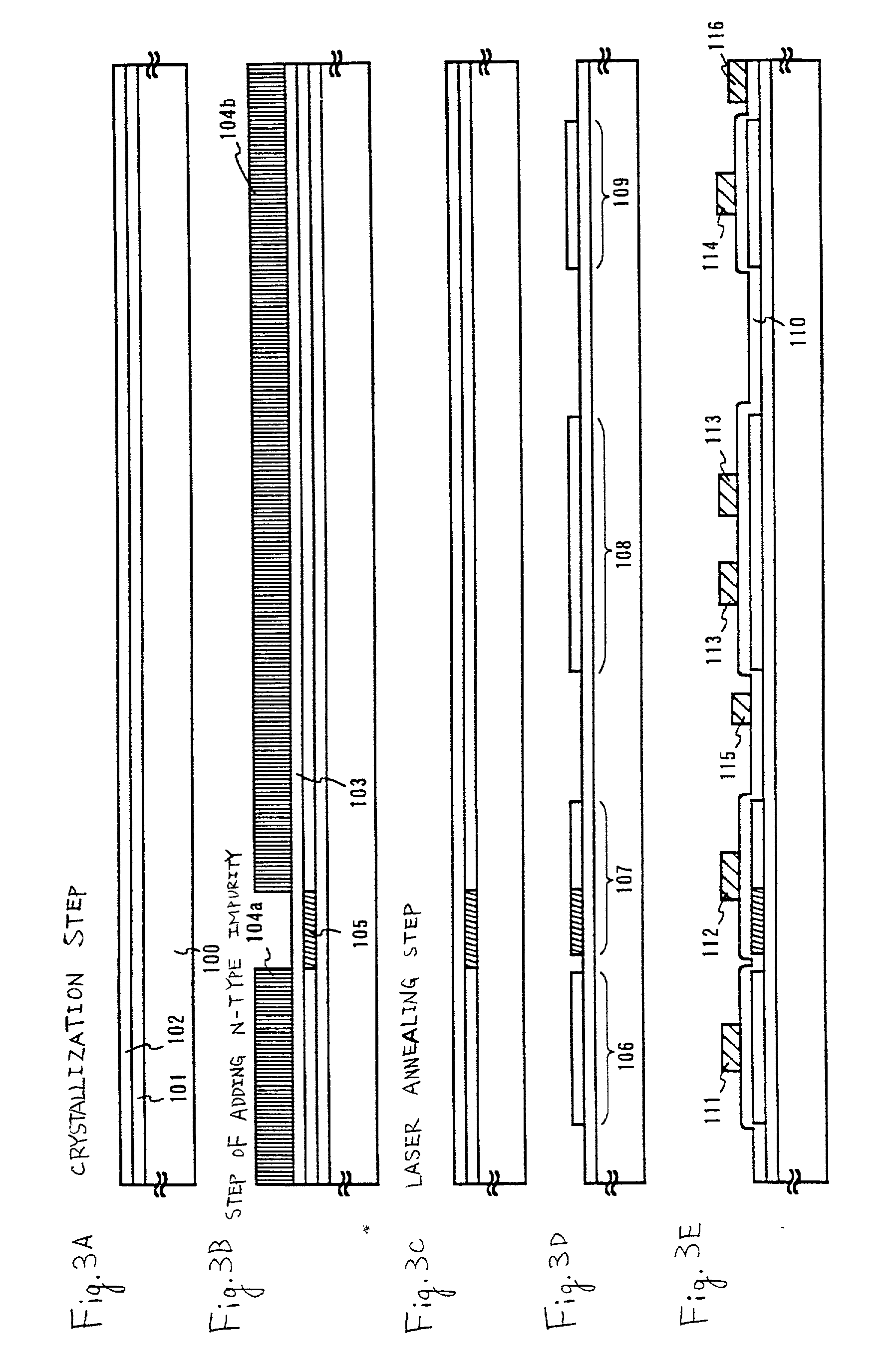
[0140] Laser crystallization is used as the means of forming the crystalline silicon film 102 in embodiment 1, and a case of using a different means of crystallization is explained in embodiment 2.
[0141] After forming an amorphous silicon film in embodiment 2, crystallization is performed using the technique recorded in Japanese Patent Application Laid-open No. Hei 7-130652. The technique recorded in the above patent application is one of obtaining a crystalline silicon film having good crystallinity by using an element such as nickel as a catalyst for promoting crystallization.
[0142] Further, after the crystallization process is completed, a process of removing the catalyst used in the crystallization may be performed. In this case, the catalyst may be gettered using the technique recorded in Japanese Patent Application Laid-open No. Hei 10-270363 or Japanese Patent Application Laid-open No. Hei 8-330602.
[0143] In addition, a TFT may be formed using the technique recorded in the sp...
embodiment 3
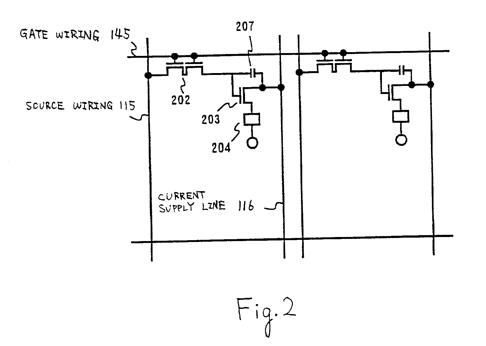
[0145] In driving the EL display device of the present invention, analog driving can be performed using an analog signal as an image signal, and digital driving can be performed using a digital signal.
[0146] When analog driving is performed, the analog signal is sent to a source wiring of a switching TFT, and the analog signal, which contains gray scale information, becomes the gate voltage of a current control TFT. The current flowing in an EL element is then controlled by the current control TFT, the EL element emitting intensity is controlled, and gray scale display is performed.
[0147] On the other hand, when digital driving is performed, it differs from the analog type gray scale display, and gray scale display is performed by time division driving. Specifically, the emitting time is adjusted to provide visual appearance that seems like changes in color gradation.
[0148] The EL element has an extremely fast response speed in comparison to a liquid crystal element, and therefore i...
embodiment 4
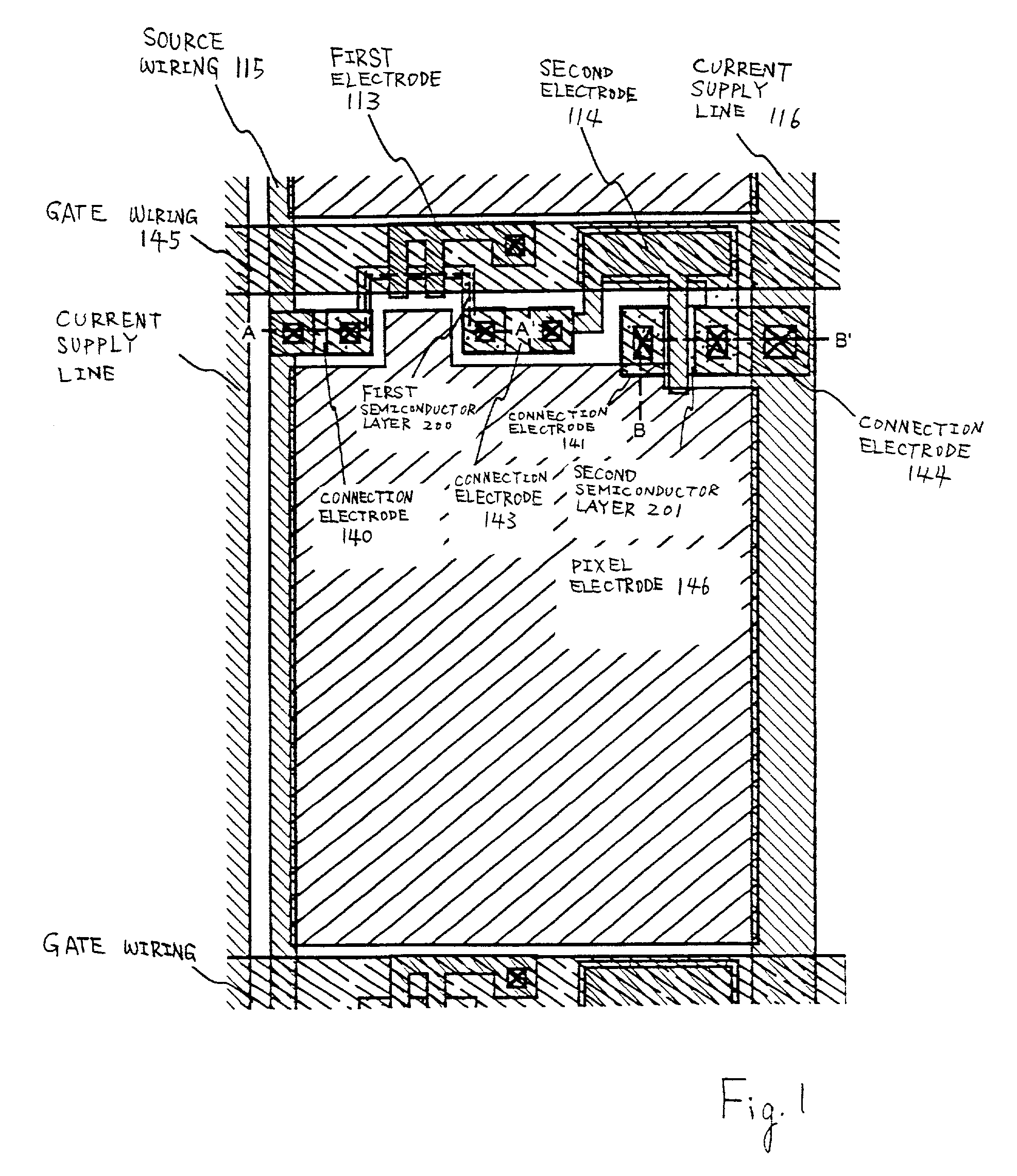
[0150] In this embodiment, a top view of a pixel structure different from that in Embodiment 1 is shown in FIG. 7A. In this embodiment, only the structure of the storage capacitor is different and other structures are substantially identical with those in Embodiment 1. Also, FIG. 7B is a cross-sectional view taken along a dotted line C-C' in FIG. 7A, and FIG. 7C shows a cross-sectional view taken along a dotted line D-D' in FIG. 7A. Parts designated by the same references correspond to those in Embodiment 1.
[0151] First, a state of FIG. 5A is obtained in accordance with Embodiment 1. However, the configuration of the second electrode is slightly different from that in Embodiment 1, and the second electrode has a portion connected to a capacitor electrode which will be formed in a later process. Then, an interlayer insulating film made of organic resin is formed and then etched to form contact holes. In this embodiment, two contact holes that reach the second electrode are formed. Al...
PUM
 Abstract
Description
Claims
Application Information