Radio frequency circuit module on multi-layer substrate

a technology of radio frequency circuit module and substrate, which is applied in the direction of cross-talk/noise/interference reduction, waveguide type devices, and association of printed circuit non-printed electric components, etc., which can solve the problems of warping, central conductors are susceptible to electromagnetic waves radiated, and poor connection degrades the electric connection sta

Inactive Publication Date: 2001-11-22
NEC CORP
View PDF0 Cites 17 Cited by
  • Summary
  • Abstract
  • Description
  • Claims
  • Application Information

AI Technical Summary

Problems solved by technology

Therefore, the central conductor is susceptible to electromagnetic waves radiated from circuit elements and wiring mounted near the central conductor or external electromagnetic noise.
Furthermore, in some cases, for example, the central conductor of the coaxial line is pulled from the outside and consequently a warp is caused in the multi-layer circuit substrate, or stress from a contained cabinet is applied to the coaxial line.
Sometimes in this case, solder peels from the pad or ground, or a metal pattern peels from the multi-layer circuit substrate, and resultant wire breaking or poor connection degrades the electric connection state.
Furthermore, there is a disadvantage that an unnecessary inductance component increases because the via is provided to connect the inner conductor, and consequently the radio frequency characteristics are degraded.
Furthermore, since the central conductor of the axial line is not connected to the inner conductor in a three-dimensional rectilinear way, the electromagnetic field near the via is disturbed and the transmission characteristics of the radio frequency signal are degraded in some cases.

Method used


Image

  • Radio frequency circuit module on multi-layer substrate
  • Radio frequency circuit module on multi-layer substrate
  • Radio frequency circuit module on multi-layer substrate

Examples


first embodiment

[0036] (First Embodiment)

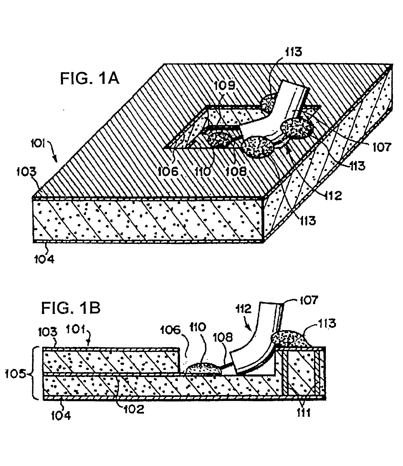
[0037] FIG. 1A is an oblique view conceptually showing a radio frequency integrated circuit module of a first embodiment according to the present invention. FIG. 1B is a sectional view of FIG. 1A in a coaxial line direction. FIG. 1B shows a radio frequency integrated circuit module having a multi-layer circuit substrate 101 with a double layer structure formed by interposing an inner conductor 102 serving as a conductor line between first ground 103 and second ground 104 which form a strip line 105.

[0038] On the first ground 103 side of the multi-layer circuit substrate 101, a cavity shaped exposed connection portion 106 is provided. In the exposed connection portion 106, the dielectric layer or the metal layer is not provided, but an exposed portion of a central conductor 108 of a semi-rigid coaxial line (hereafter referred to as "coaxial line") 107 is fixed in such a manner that the coaxial line 107 is not affected by electromagnetic waves generated from c...

second embodiment

[0050] (Second Embodiment)

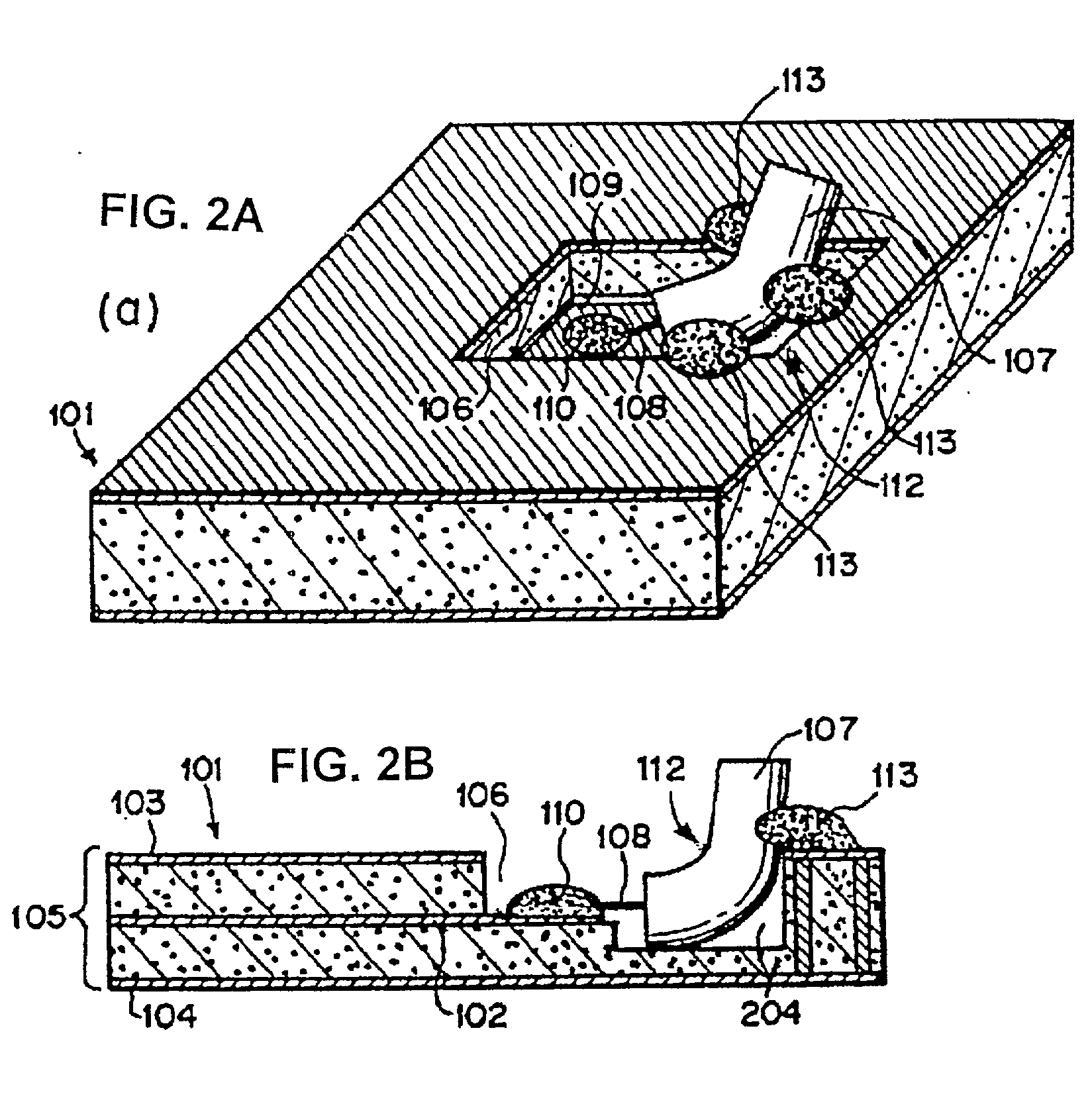
[0051] FIG. 2A is an oblique view conceptually showing a radio frequency integrated circuit module of a second embodiment according to the present invention. FIG. 2B is a sectional view of FIG. 2A in a coaxial line direction. In FIG. 2A, numeral 204 denotes an exposed connection portion provided in order to structurally make it hard to burden a load on the coaxial line 107. In FIG. 2A, the same components as those shown in FIG. 1A are denoted by like characters.

[0052] In the present embodiment, a step between an exposed connection portion 106 and an exposed connection portion 204 is set equal to the radius of an outer conductor 112. As a result, the stress caused by bending the coaxial line 107 is eliminated. In its turn, the load applied to solder 113 can be reduced. It becomes possible to make the solder 113 hard to peel from the first ground 103. As compared with the radio frequency integrated circuit module shown in FIG. 1A, therefore, degradation of el...

third embodiment

[0053] (Third Embodiment)

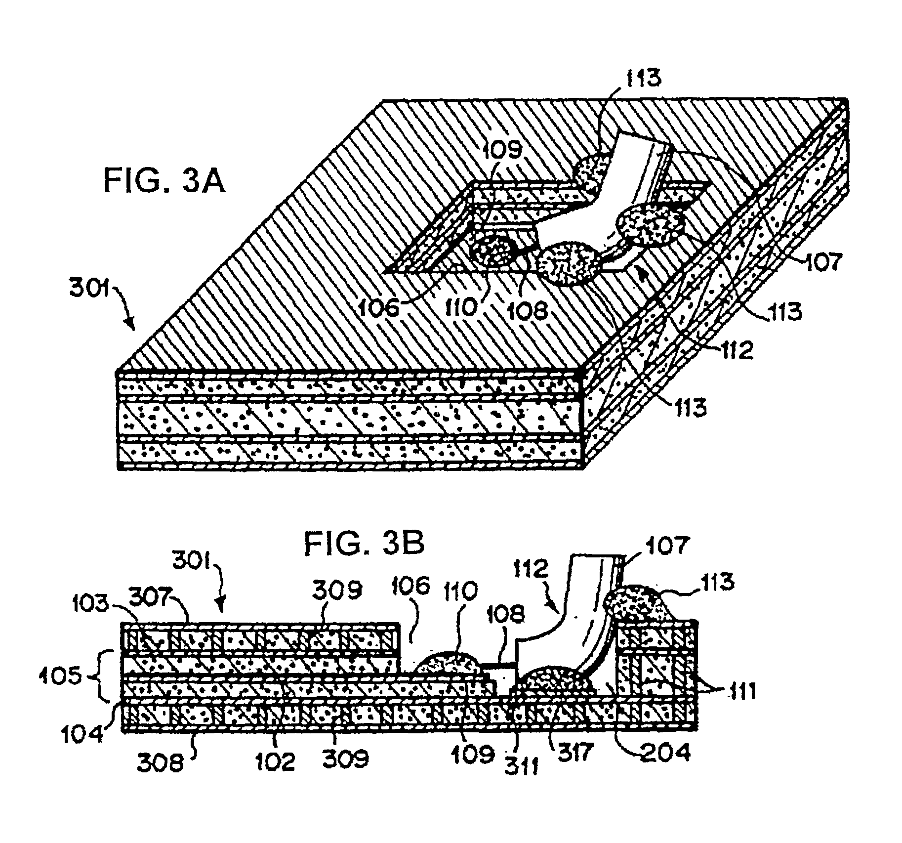
[0054] FIG. 3A is an oblique view conceptually showing a radio frequency integrated circuit module of a third embodiment according to the present invention. FIG. 3B is a sectional view of FIG. 3A in a coaxial line direction. In the present embodiment, a multi-layer circuit substrate 301 of a five layer structure is used.

[0055] In FIG. 3A, numerals 307, 308 and 311 denote third to fifth grounds. Numerals 309 denote vias provided at a high density in a two dimensional way to connect the first and third grounds together and connect the second and fourth grounds together. Numeral 317 denotes solder for connecting an outer conductor 112 to the fifth ground 311.

[0056] In FIG. 3A, the same portions as those shown in FIG. 2A are denoted by like characters. The present embodiment has been described by taking the case where the fifth ground 311 is provided, as an example. However, the outer conductor 112 and the second ground 104 may be directly connected together by ...


PUM


Abstract

An object of the present invention is to provide a radio frequency integrated circuit module that is less susceptible to the electromagnetic influence and that is not degraded in electric connection. The radio frequency circuit module of the present invention including circuit elements mounted on a multi-layer circuit substrate having dielectric layers is characterized in that an exposed connection portion is provided by removing a part of the dielectric, and a strip line connected to said circuit elements and a co-axial line for transmitting a radio frequency signal from/to said strip line are connected together in a bottom portion of said exposed connection portion so as to be rectilinear in a three dimensional way.

Description

[0001] 1. Technical Field of the Invention[0002] The present invention relates to a radio frequency circuit module, such as monolithic radio frequency integrated circuit module or a hybrid microwave integrated circuit module, formed by mounting circuit elements on a circuit substrate having dielectric layers for a module and a communication apparatus using the radio frequency circuit.[0003] 2. Description of the Prior Art[0004] Heretofore, there is a radio frequency integrated circuit module having a multi-layer circuit substrate, on which circuit elements such as active elements including transistors and diodes and passive elements including resistors and inductors, and wiring for mutually connecting the circuit elements are mounted. When radio frequency integrated circuit module are mutually connected, a transmission path having a high shield property, such as a coaxial line, is used between transmission and reception terminals in many cases.[0005] FIG. 16A is an oblique view conc...

Claims


Application Information

Patent Timeline
Patent Type & Authority Applications(United States)
IPC IPC(8): H01P5/08H05K1/02H05K1/18H05K3/34
CPCH01P5/085H05K1/0219H05K1/183H05K3/3405H05K3/341H05K3/3421H05K2201/09809H01L2924/19107H05K2201/09845H05K2201/10356H01L2924/0002H01L2924/00H05K9/00
Inventor TAMAKI, NAOYAMASUDA, NORIO
Owner NEC CORP
Why Eureka
Try Eureka