Multi-functional I/O buffers in a field programmable gate array (FPGA)
- Summary
- Abstract
- Description
- Claims
- Application Information
AI Technical Summary
Problems solved by technology
Method used
Image
Examples
Embodiment Construction
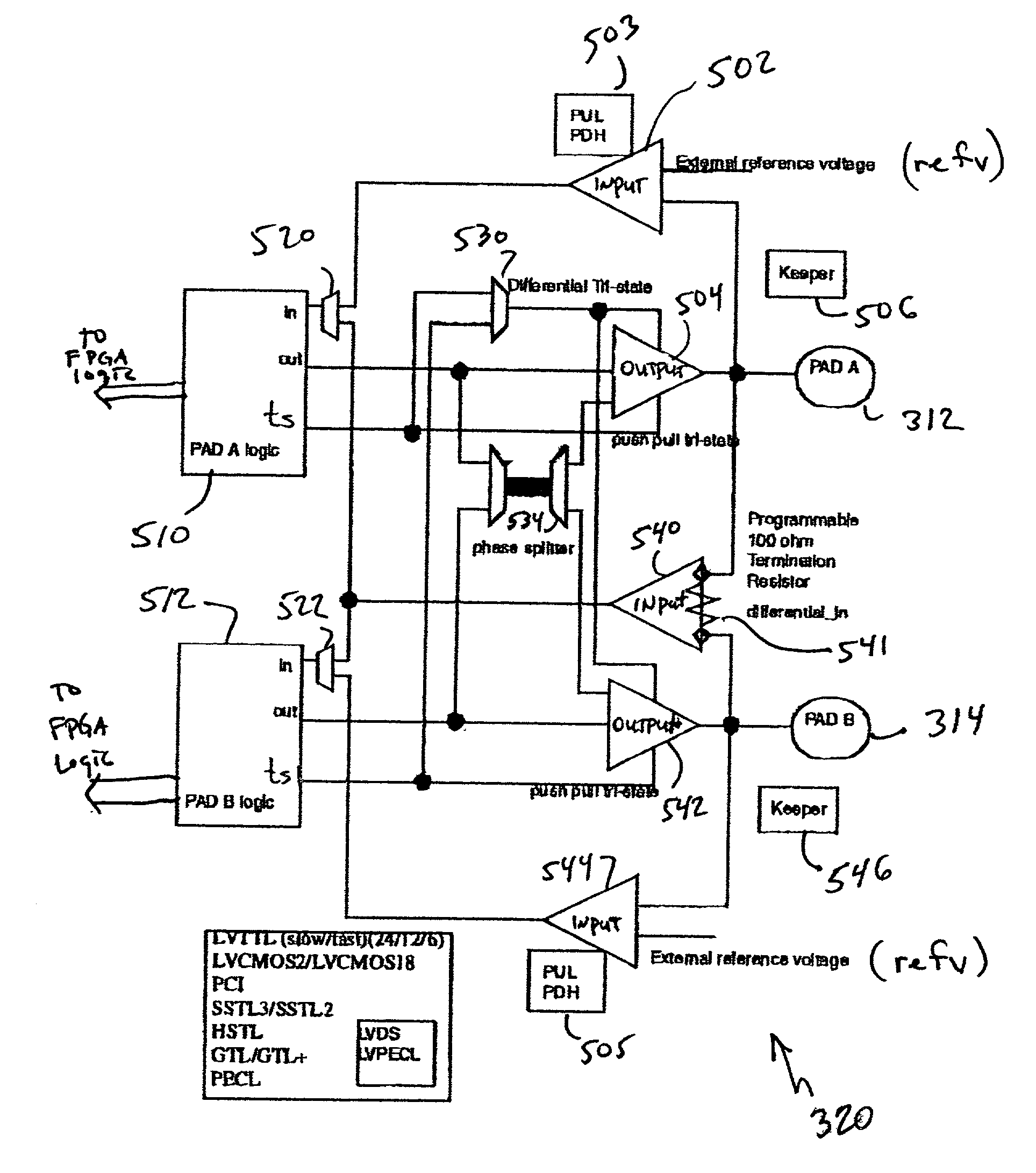
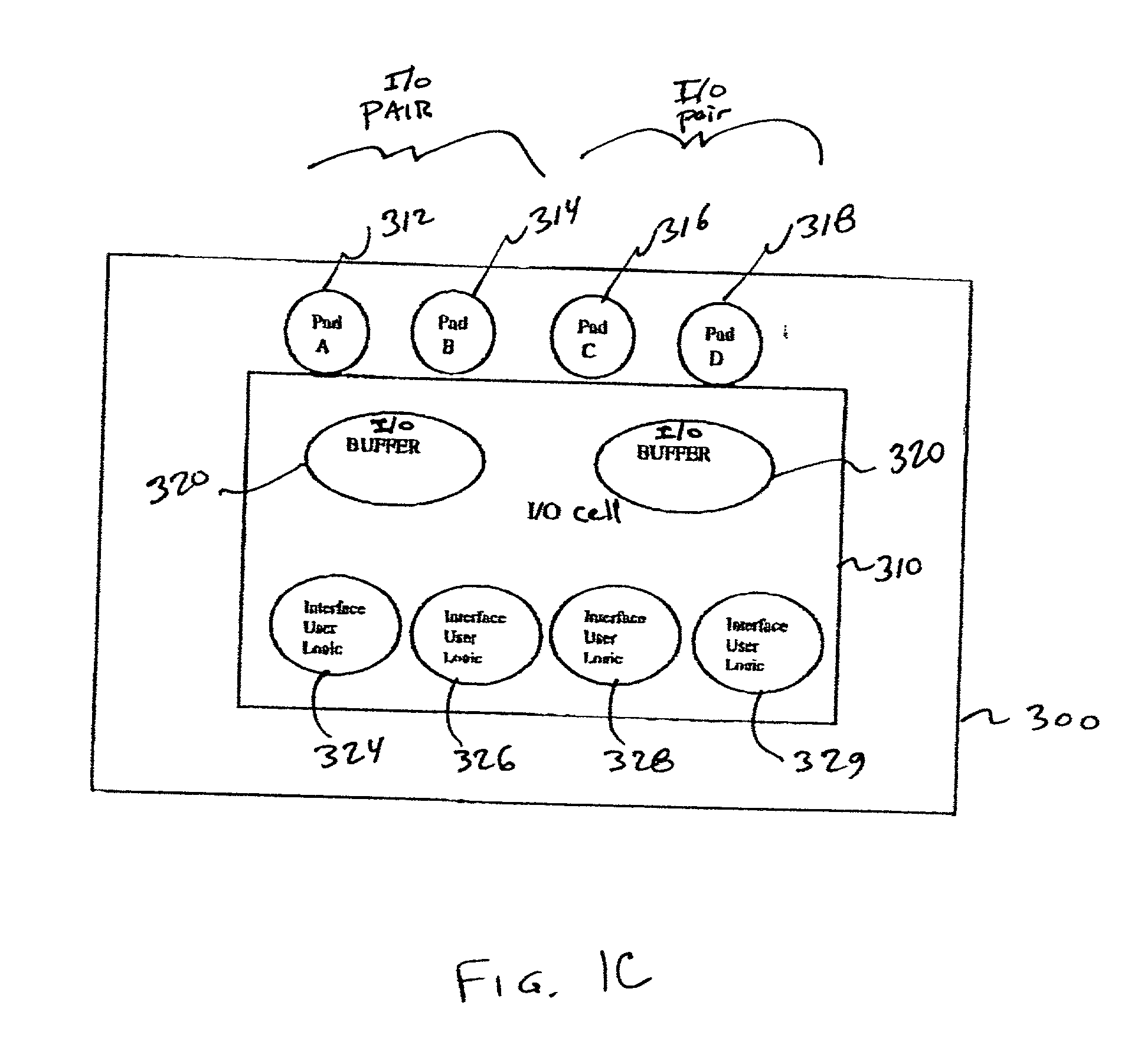
[0037] The present invention relates to the provision of a multi-functional programmable I / O buffer in a Field Programmable Gate Array (FPGA) device. The I / O buffer is programmably configurable to meet any of a wide range of I / O standards, be it single ended or differential, 5V, 3.3.V, 2.5V or 1.5V logic, without the need for implementing multiple I / O buffers to properly handle each different iteration of I / O requirements.
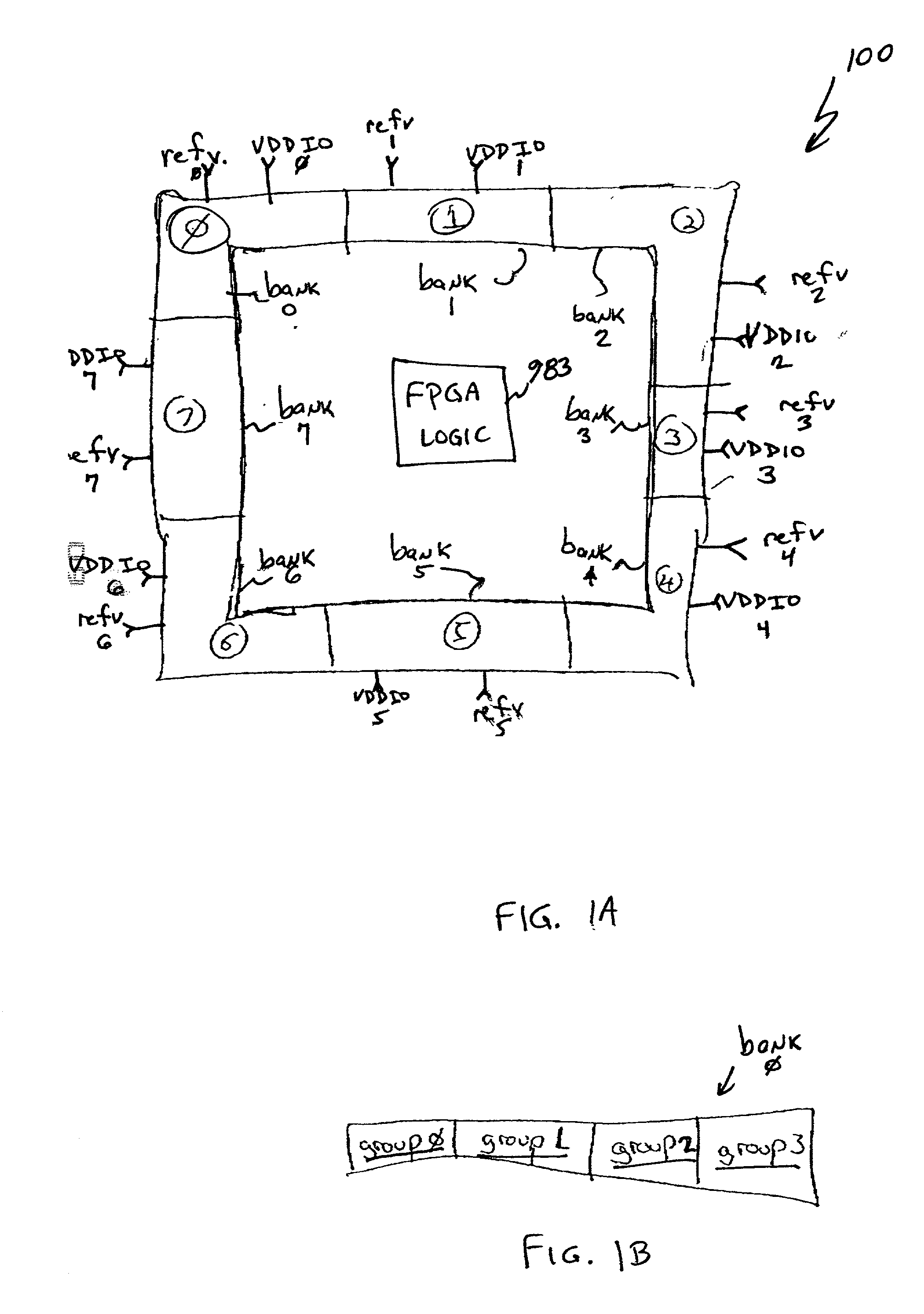
[0038] In accordance with the principles of the present invention, a high-speed I / O interface is provided which includes an embedded, internal programmable resistor (e.g., a programmable 100 ohm resistor) for use in differential I / O applications, thus eliminating the conventional requirement for the use of an external resistor connected to each differential receiver I / O pin. The present invention also separates I / O pads into groups in each of a plurality of banks in a programmable device (e.g., PLD, FPGA, etc.), with each group being separately powered by the user....
PUM
 Abstract
Description
Claims
Application Information


