Double data rate input and output in a programmable logic device

a logic device and input and output technology, applied in the field of field programmable gate arrays, can solve the problems of reducing the signal integrity of the receiver, increasing the cost of the user's use of external resistors, and each of these dedicated i/o buffers offers little flexibility to perform in other capacities

Inactive Publication Date: 2002-01-10
LATTICE SEMICON CORP
View PDF0 Cites 17 Cited by
  • Summary
  • Abstract
  • Description
  • Claims
  • Application Information

AI Technical Summary

Problems solved by technology

Unfortunately, use of an external resistor increased costs to the user.
Moreover, signal integrity is dependent on the proximity of the termination resistor to the receiver, and thus external resistance reduces signal integrity at the receiver.
However, each of these dedicated I/O buffers

Method used


Image

  • Double data rate input and output in a programmable logic device
  • Double data rate input and output in a programmable logic device
  • Double data rate input and output in a programmable logic device

Examples


Embodiment Construction

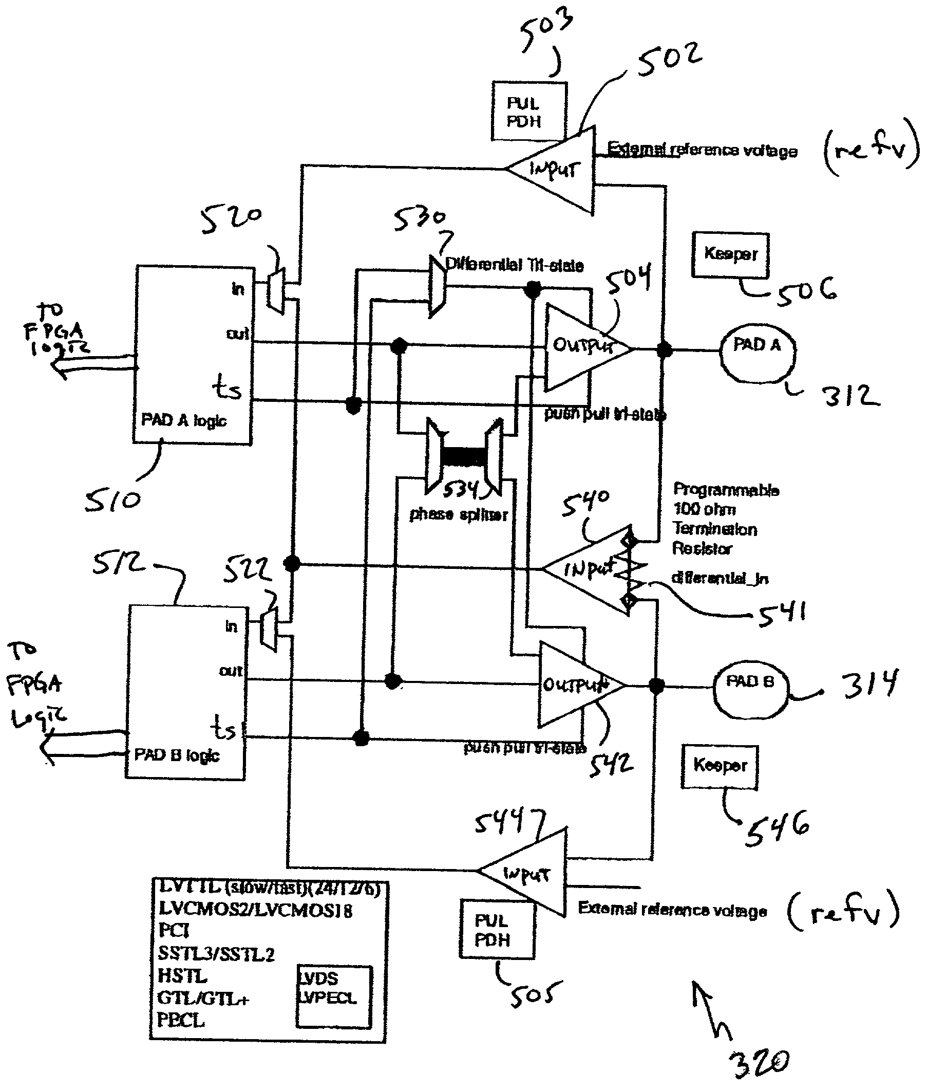
[0037] The present invention relates to the provision of a multifunctional programmable I / O buffer in a Field Programmable Gate Array (FPGA) device. The I / O buffer is programmably configurable to meet any of a wide range of I / O standards, be it single ended or differential, 5V, 3.3V, 2.5V or 1.5V logic, without the need for implementing multiple I / O buffers to properly handle each different iteration of I / O requirements.

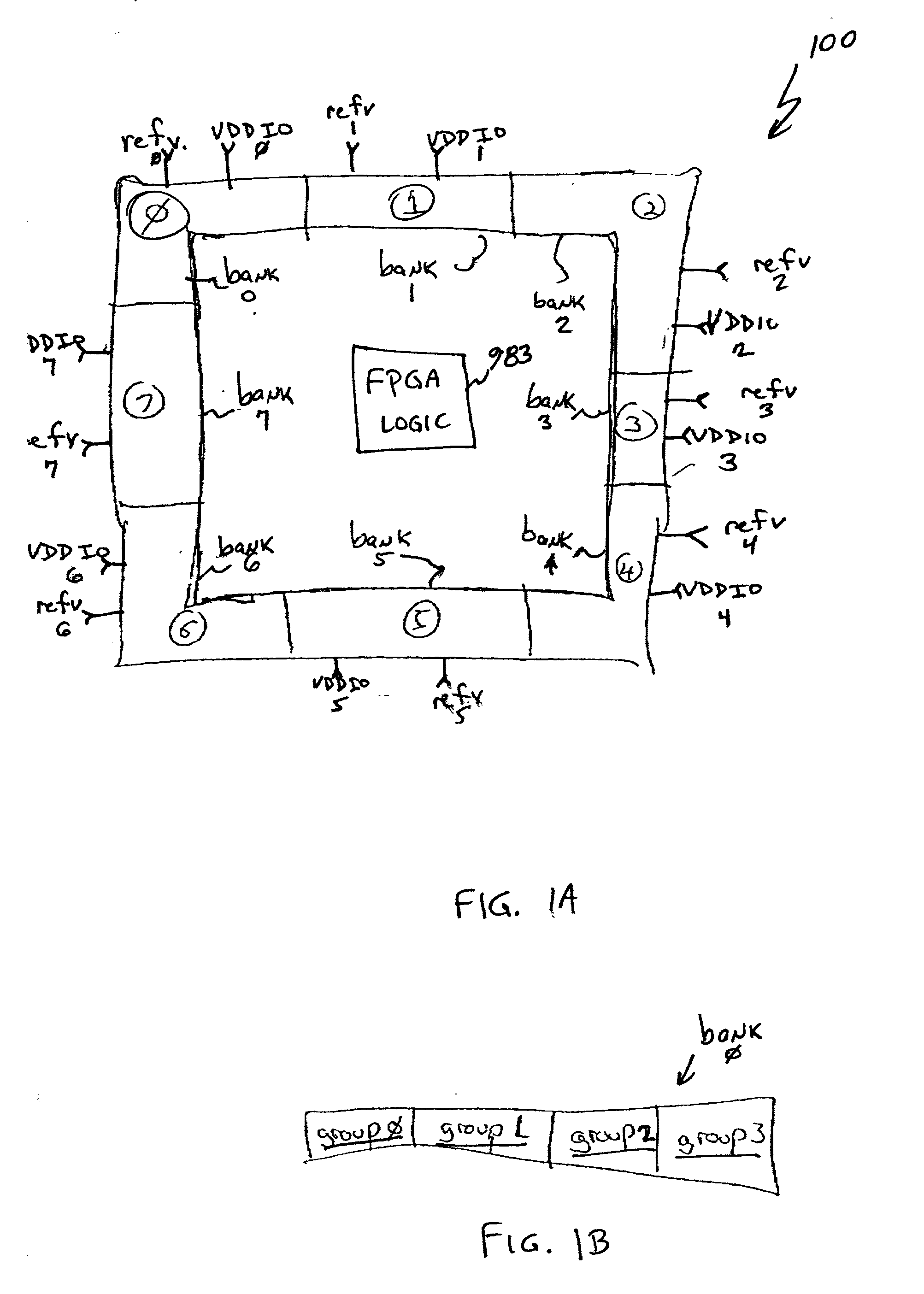
[0038] In accordance with the principles of the present invention, a high-speed I / O interface is provided which includes an embedded, internal programmable resistor (e.g., a programmable 100 ohm resistor) for use in differential I / O applications, thus eliminating the conventional requirement for the use of an external resistor connected to each differential receiver I / O pin. The present invention also separates I / O pads into groups in each of a plurality of banks in a programmable device (e.g., PLD, FPGA, etc.), with each group being separately powered by the user. I...


PUM


Abstract

A multi-functional programmable I/O buffer in a Field Programmable Gate Array (FPGA) device. The I/O buffer is programmably configurable to meet any of a wide range of I/O standards, be it single ended or differential, 5V, 3.3V, 2.5V or 1.5V logic, without the need for implementing multiple I/O buffers to properly handle each different iteration of I/O requirements. An embedded, internal programmable resistor (e.g., a programmable 100 ohm resistor) is programmably selected for use in differential I/O applications, thus eliminating the conventional requirement for the use of an external resistor connected to each differential receiver I/O pin. The present invention also separates I/O pads into groups in each of a plurality of banks in a programmable device (e.g., PLD, FPGA, etc.), with each group being separately powered by the user. The disclosed multi-functional I/O buffer may be programmably configured by the user to be, e.g., a single ended receiver or transmitter, a reference receiver or transmitter, or a differential receiver or transmitter. The pad logic of the multi-functional I/O buffer may include a double data rate input and output mode, each of which includes two flip-flop devices operating on opposite sides of a data clock signal. One of the two flip-flop devices may be borrowed from another logic element, e.g., from a shirt register logic element.

Description

[0001] This application claims priority from U.S. Provisional Application No. 60 / 207,371 entitled "Novel Field Programmable Gate Array" filed on May 26, 2000, the specification of which is hereby expressly incorporated herein by reference.[0002] 1. Field of the Invention[0003] This invention relates generally to field programmable gate arrays (FPGAs). In particular, it relates to the implementation of improved architectures and functions to interface with an FPGA.[0004] 2. Background of Related Art[0005] A Field Programmable Gate Array (FPGA) is a programmable integrated circuit which provides a customized logic array and functionality to a particular customer.[0006] FIG. 8 depicts a conventional Field Programmable Gate Array (FPGA).[0007] In particular, as shown in FIG. 8, an FPGA 400 typically includes four distinct features: configuration memory 406, input / output (I / O) blocks 408-414, configurable logic blocks 404, and a routing network 402 between the internal components.[0008] ...

Claims


Application Information

Patent Timeline
IPC IPC(8): G06F1/10G06F13/36G06F13/20H01L21/82H01L21/822H01L27/04H03K5/13H03K19/0175H03K19/173H03K19/177H03L7/081H03L7/099
CPCG06F1/10H03K5/13H03K19/017581H03K19/17732H03K19/17736H03K19/1774H03K5/133H03K19/17748H03K19/1776H03K19/17788H03K19/17792H03L7/081H03L7/0996H03K19/17744
Inventor ANDREWS, WILLIAM B.BRITTON, BARRY K.
Owner LATTICE SEMICON CORP
Why Eureka
Try Eureka