Gaseous-based radiation detector and apparatus for radiography
- Summary
- Abstract
- Description
- Claims
- Application Information
AI Technical Summary
Problems solved by technology
Method used
Image
Examples
first embodiment
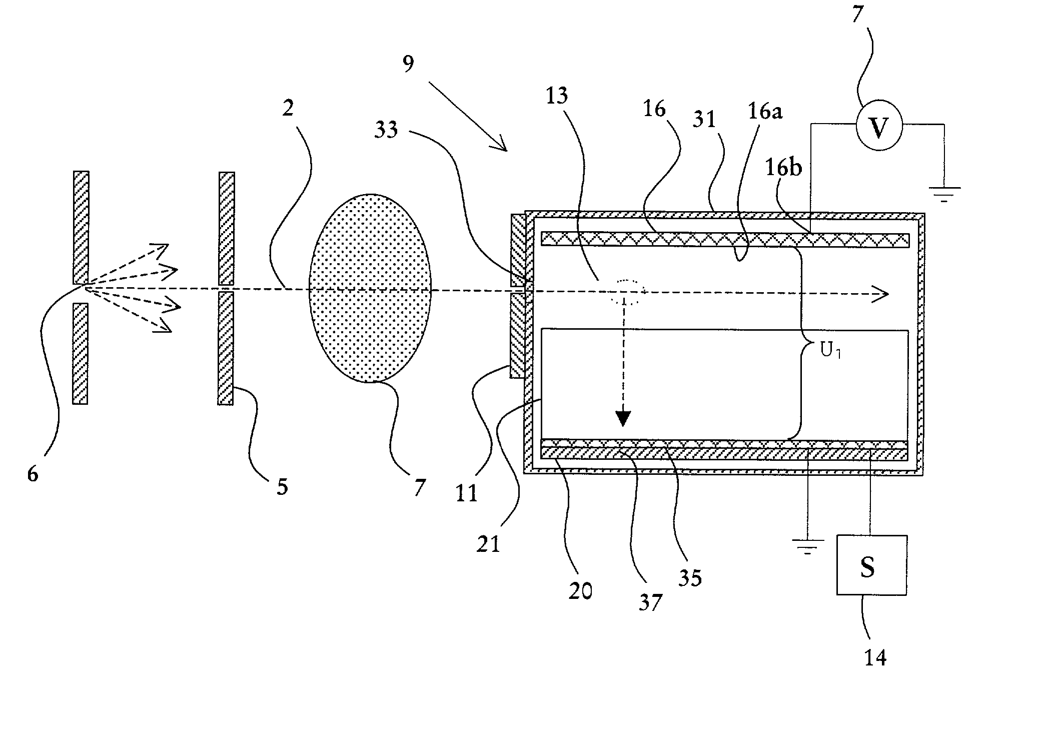
[0023] FIG. 1 is a sectional view in a plane orthogonal to the plane of a planar fan-shaped X-ray beam 2 of a device for planar beam radiography, according to the present invention. The device includes an X-ray source 6, which together with a first thin collimator window 5 produces the planar X-ray beam 2, for irradiation of an object 7 to be imaged.
[0024] The beam transmitted through the object 7 enters a detector 9. Optionally a thin slit or second collimator window 11, which is aligned with the X-ray beam, forms the entrance for the X-ray beam 2 to the detector 9.
[0025] The detector 9 is oriented such that the X-ray photons can enter sideways between a cathode arrangement 16 and an anode arrangement 20 between which a space 13 capable of being filled with an ionizable gas or gas mixture is arranged. By means of a high voltage DC supply unit 7 a voltage U.sub.1 can be applied between cathode 16 and anode 20 for drift of electrons and ions in space 13. Cathode 16 and anode 20 arran...
fifth embodiment
[0056] FIG. 5 shows schematically a portion of a cross sectional view of a detector according to the invention. The detector comprising a cathode electrode 72 including a resistive or semiconducting substrate 75 and a conductive layer 76 and an anode 1 including a dielectric substrate 3 and a conductive layer 4 being an anode electrode. Between the electrodes a space 13 filled with an ionizable gas and an electron avalanche amplification arrangement 17 is arranged, the amplification arrangement 17 including an avalanche amplification cathode 18 and an avalanche amplification anode 19, separated by a dielectric 24. (Here, the anode 4 and the avalanche amplification anode 19 are the very same piece of element.) The dielectric 24 could be a gas or a solid substrate 24 carrying the cathode 18 and the anode 19, as shown in FIG. 5. Both, or one, of the cathode 18 and the anode 19 can be provided with a resistive or semiconducting layer on top of a conductive layer so that a surface of the...
sixth embodiment
[0060] FIG. 6 shows schematically a portion of a cross sectional view of a detector according to the invention. This embodiment differs from the embodiment according to FIG. 5 in that the anode electrodes 4 / 19 are formed by different conductive elements, being spaced by a dielectric, which could be solid or a gas, and that the openings or channels also are formed in the avalanche anode electrode 19. The avalanche amplification anode 19 is connected to the DC power supply 7. In the case the dielectric between the anode electrodes 4 and 19 is solid, it includes openings or channels through the dielectric, the openings or channels essentially corresponding the openings or channels forming the avalanche regions 25. An electric field is created between the anode electrodes 4 and 19. This field could be a drift field, i.e. a weaker field, or an avalanche amplification field, i.e. a very strong electric field.
[0061] Any or all of the cathode 72, 18 and the anode 4, 19 electrodes can be pro...
PUM
 Abstract
Description
Claims
Application Information


