
Data object architecture and method for xDSL ASIC processor

a data object and processor technology, applied in the field of data object architecture and method of xdsl asic processor, can solve the problems of large gate count, difficult and costly feature upgrade path, functional units not being able to interrelate or even simultaneously operate,

Inactive Publication Date: 2002-01-24
REALTEK SEMICON CORP
View PDF61 Cites 2 Cited by
  • Summary
  • Abstract
  • Description
  • Claims
  • Application Information

AI Technical Summary

Benefits of technology

[0132] As a result, the EMKG of an ASIC block may be higher than otherwise expected or evaluated by conventional analysis, because it can be multiplied in some instances by a time sharing factor Tf, resulting in a net EMKG proportional to TF*EMKG. Again, the applicant believes that this principle can be easily and beneficially extended by skilled artisans to other environments other than xDSL applications.
[0146] Using the above innovations, the applicant projects that an ASIC transistor count per ADSL port can be significantly reduced down to 1 million transistors per port, compared to is 6 to 7 million transistors per port in a typical ASIC design. This number allows a practical and cost-effective 16-port design in a single conventional 0.18 .mu.m based chip design.

Problems solved by technology

A transceiver design involving only ASIC components will necessarily require at least one distinct logic core for every operation contemplated, resulting in a large gate count, and a difficult and costly feature upgrade path.
This approach involves a series of separate collections of gates that are permanently wired, and the functional units are not capable of interrelation or even simultaneously operation.
All of these approaches involve significant flexibility and relatively low power.
However, the FPGA approach typically results in an undesirable quantity of unused gates, and a relatively slow speed due to reconfiguration time and the inherent slowness of a software design.
Furthermore, the receive task and the transmit task require differing amounts of the computing resources.
1. The same architecture for a varying number of ADSL ports. This minimizes the effort in re-engineering for a different port design.
2. Minimal transistors count per port. Compared to a typical ASIC design, this new architecture reduces the required transistors count from 6M per port to less than 1M per port. This minimal count design results in a tremendous cost, power, and space saving.
3. Programmable design that allows different ADSL implementations in different regions and future standards.
4. Power management to reduce the total power dissipation as the ADSL line rate decreases. This is a very important feature for central-office applications.
5. Configurable operations. For example, with the scalable architecture, a single 2-port ADSL chip solution can be configured as (1) one-port ADSL-Transceiver-Unit-Remote (ATU-R), (2) one-port ATU-Central-Office (ATU-C), (3) two-port ATU-R, (4) two-port ATU-C, and (5) one-port ATU-C and one-port ATU-R. The last one can be used as a single chip solution for ADSL repeaters. Similarly, another single chip can be configured as 2, 4, 8, or 16-port ATU-C.
6. Standalone system-on-chip design. This provides the easiest way for system integration. There is no dependence on other processors. Standard interfaces such as Utopia are provided for the external requirements.
7. System integration in a single chip. With a minimal transistor count design, it also allows for single-chip design with other system function such as voice over DSL (VoDSL), IP packet routing, and ATM cell switching.
A 16-port solution will thus require 6400 MIPS, which is impractical for any single DSP, and is incompatible with power dissipation and similar cost issues.

Method used


Image

  • Data object architecture and method for xDSL ASIC processor
  • Data object architecture and method for xDSL ASIC processor
  • Data object architecture and method for xDSL ASIC processor

Examples


Embodiment Construction

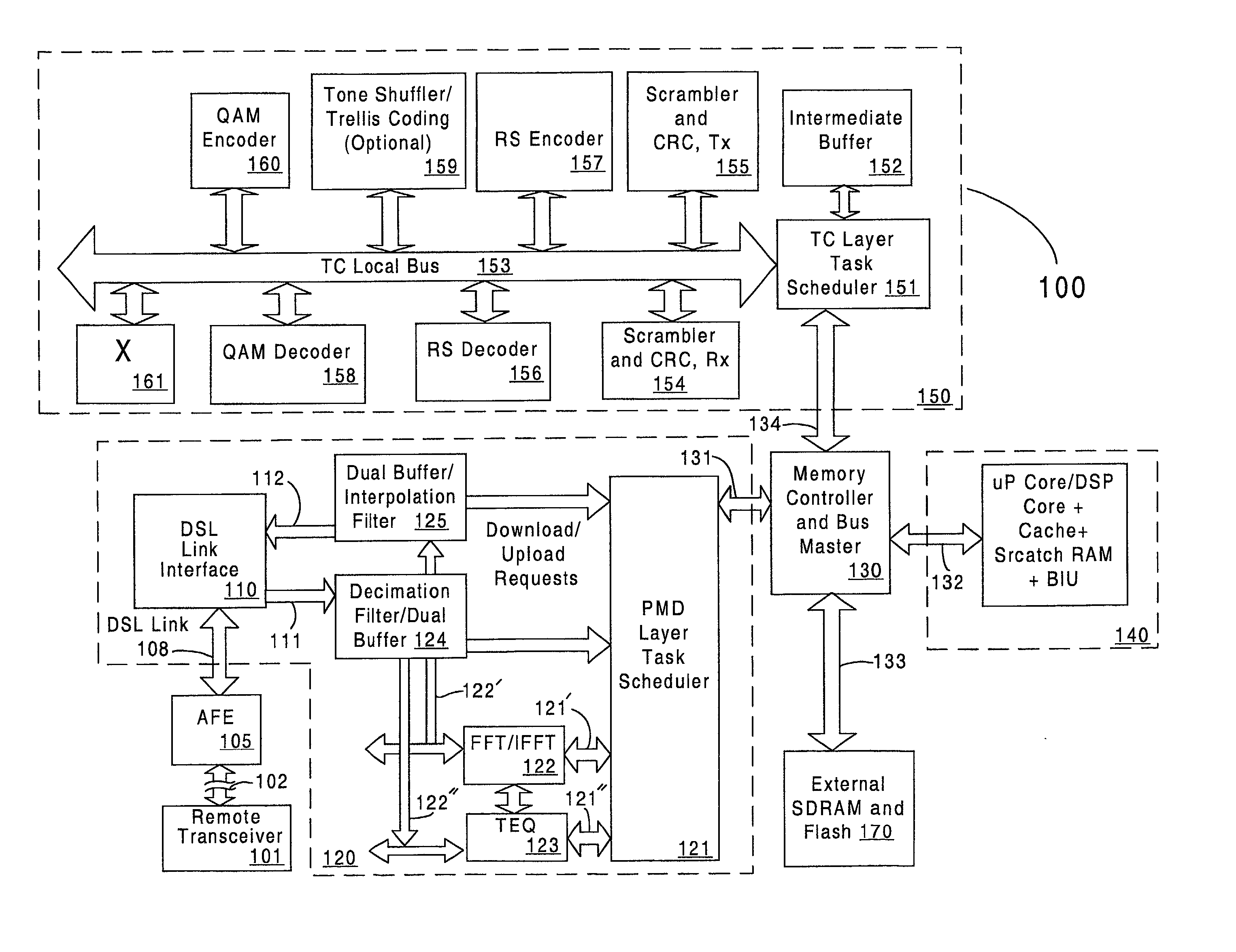
[0148] A block diagram of the hardware elements used in a preferred multi-port embodiment of the present system is shown in FIG. 1. It will be understood by those skilled in the art that some non-material aspects of the system shown in FIG. 1 have been simplified and / or omitted in order to better explain the scope of the present invention. Furthermore, while aspects of the present invention are explained by reference to such preferred embodiment and other specific architectural implementation details, the scope of the present invention is by no means limited to any embodiments and details discussed herein, and many other variations, additions, modifications, etc. will be apparent to those skilled in the art from the present disclosure.

[0149] A scalable architecture system 100 as described herein includes three major subsystems: (1) PMD 120 (2) TC 150 and (3) microprocessor / DSP 140. The first two subsystems consist of ASIC modules to perform part of the ADSL / ATM PMD and TC functions....


PUM


Abstract

A structure for a data object is disclosed with a field and format structure optimized for use by a set of pipeline stages that are interconnected logically through a common pipeline memory. The data object includes both a first portion containing data relating to one or more of a plurality of parameters associated with the control and / or the configuration of one or more processing circuitry blocks, and a second portion containing data associated with computations performed by the processing circuitry blocks. Other portions contain both general and specific types of operational control information used by the processing circuitry blocks. The data object acts as a form of common data exchange mechanism between disparate types of pipeline stages, including in hybrid (mixed) software-hardware pipelines. The control data in the data object can be used by a first pipeline stage to affect or adaptively change operational functioning of downstream pipeline stages.

Description

[0001] The present inventions relate to data exchange mechanisms for a communications system, and more particularly to a type of data object that is used as an input / output mechanism for a set of interleaved hardware / software pipeline stages.[0002] ADSL is being widely deployed around the world as a major broadband Internet access technology. As the number of ADSL subscribers and the demand for bandwidth rapidly increase, it is highly desirable to provide a multiple-port ADSL solution that has a high density, low power, low gate count, and can be incorporated in a single chip for both central-office (CO) side and customer premises (CPE) side applications. To try to obtain these features in a communications transceiver, a designer typically looks at many trade-offs associated with using various approaches to signal processing. Several prior art techniques have involved using a digital signal processor (DSP), an application-specific integrated circuit (ASIC), or a field-programmable g...

Claims


Application Information

Patent Timeline
Patent Type & Authority Applications(United States)
IPC IPC(8): H04J99/00G06F1/04G06F1/12G06F3/00G06F5/06G06F9/38G06F13/00G06F13/38G06F15/00G06F15/16G06F15/76H04L1/00H04L12/28H04L12/56H04L12/64H04L27/26H04M11/06
CPCG06F9/3867H04L1/0043H04L1/0052H04L12/2856H04L12/289H04L27/2601H04L27/2626H04L27/2647H04L2012/5665H04L2012/6478H04M11/062Y02B60/36Y02D30/50
Inventor LIU, MING-KANG
Owner REALTEK SEMICON CORP
Learn More