Semiconductor device and manufacturing method therefor

a semiconductor and manufacturing method technology, applied in the direction of organic semiconductor devices, discharge tubes/lamp details, discharge tubes luminescnet screens, etc., can solve the problems of increased production costs, high-performance light-emitting devices using plastic films, and high cost of circular polarizing films

Inactive Publication Date: 2002-03-14
SEMICON ENERGY LAB CO LTD
View PDF12 Cites 85 Cited by
  • Summary
  • Abstract
  • Description
  • Claims
  • Application Information

AI Technical Summary

Benefits of technology

[0011] Furthermore, an object of the present invention is to provide a low cost EL light emitting device in which the cost of manufacturing the EL light emitting device is reduced by preventing the EL light emitting device from being made into a mirrored surface without using a circular polarizing film.

Problems solved by technology

TFTs having electrical properties nearly as good as those of TFTs formed on glass substrates cannot be formed at present without lowering the maximum process temperature because the heat resistance of plastic films is low.
High performance light emitting devices using plastic films have therefore not been achieved.
However, outside light 17 (light from outside the light emitting device) made incident to pixels which do not generate light is reflected by the rear surface of the anode (the surface contacting the light emitting layer), and there is a problem in that the rear surface of the cathode acts as a mirror and the external environment is shown on the observation surface (surface pointed toward an observer).
Further, in order to avoid this problem, there is a method in which a circular polarizing film is attached to the observation surface of the EL light emitting device so that the external environment is not shown on the observation surface, but the circular polarizing film is extremely expensive, and thus invites a further problem of an increase in production costs.

Method used


Image

  • Semiconductor device and manufacturing method therefor
  • Semiconductor device and manufacturing method therefor
  • Semiconductor device and manufacturing method therefor

Examples


embodiment 1

[0059] [Embodiment 1]

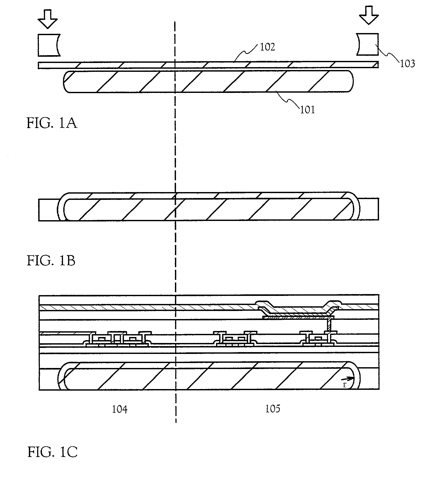
[0060] An example of a method of manufacturing a light emitting device sandwiched by an element substrate made from a thin metallic substrate, and by a fixing substrate made from a resin substrate, is shown in embodiment 1 using FIGS. 1A to 1C, and FIGS. 2A and 2B. Note that the present invention is of course not limited by the structure shown in embodiment 1.

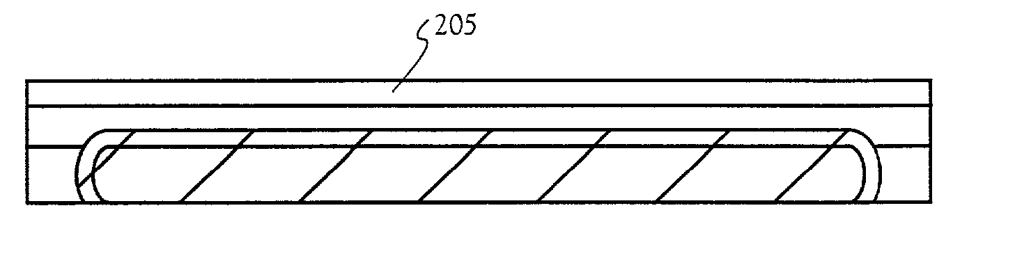
[0061] First, a stainless steel substrate (JIS SUS304 or JIS SUS316) is used as the substrate holder 101. The substrate holder 101 and the element forming substrate 102, made from a thin metallic substrate (JIS SUS304 or JIS SUS316), are then fixed together by the fixing portion 103. (See FIG. 1B.)

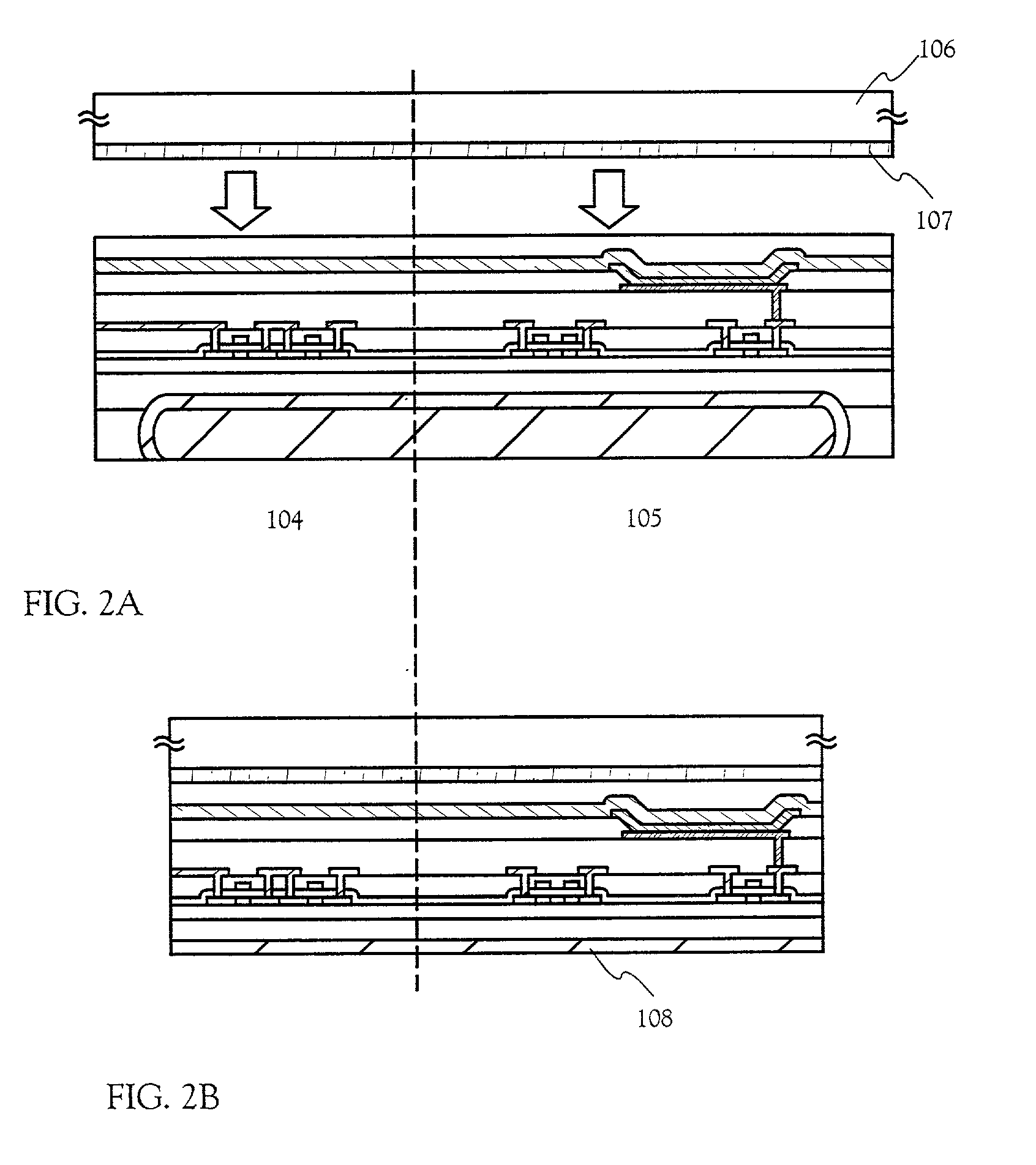
[0062] After next forming a base insulating film on the metallic substrate 102, necessary elements are formed on the base insulating film. An example in which the driver circuit 104 and the pixel portion 105 having EL elements are formed is shown here. (See FIG. 1C.)

[0063] A silicon oxide film, a silicon nitride f...

embodiment 2

[0076] [Embodiment 2]

[0077] A method of selectively forming a crystalline semiconductor film using a metallic element for promoting crystallization of an amorphous semiconductor film is explained using FIGS. 3A to 3C. Reference numeral 200 denotes a base insulating film, as discussed above, in FIG. 3A.

[0078] First, a metallic substrate and a substrate holder are fixed by a fixing portion in accordance with the method shown in the embodiment mode, and the base film 200 is formed thereon. An amorphous silicon film 201 is then formed on the base insulating film 200 by a known method. A 150 nm thick silicon oxide film 202 is then formed on the amorphous silicon film 201. No limitations are placed on the method of manufacturing the silicon oxide film, and it may be formed, for example, by high frequency (13.56 MHz) emission with a power density of 0.5 to 0.8 W / cm.sup.2 using a mixture of tetraethyl orthosilicate (TEOS) and O.sub.2, and at a reaction pressure of 40 Pa and a substrate temp...

embodiment 3

[0082] [Embodiment 3]

[0083] Metallic elements utilized in crystallization of a crystalline silicon film manufactured by performing the processes explained by embodiment 2 remain after manufacture. Even if the metallic elements are not distributed evenly within the film, they exist at a concentration exceeding 1.times.10.sup.19 / cm.sup.3 when taking an average concentration. It is of course possible to use the crystalline semiconductor film in channel forming regions for all types of semiconductor devices such as TFTs, in this state, but it is very preferable to remove the metallic elements by gettering.

[0084] An example of a gettering process is explained using FIGS. 4A to 4C. A silicon oxide film mask 302 having a thickness of 150 nm is formed on the surface of a crystalline silicon film 301, an opening portion 303 is formed, and a region in which the crystalline silicon film is exposed is formed. It is possible to utilize the silicon oxide film 202 shown by FIG. 3A as is for a case...


PUM

PropertyMeasurementUnit
thicknessaaaaaaaaaa
surface roughnessaaaaaaaaaa
temperatureaaaaaaaaaa

Abstract

A light weight and a low cost EL display device is provided, in which light emitting elements are formed on a flexible film. A thin metallic substrate is used as an element forming substrate with the present invention, edge portions of the metallic substrate are bent, and the metallic substrate is attached with good adhesion, within a vacuum, to a substrate holder which possesses curvature in its edge portions. After then forming light emitting elements on the thin metallic substrate, the substrate holder is separated.

Description

[0001] 1. Field of the Invention[0002] The present invention relates to a device (hereafter referred to as a light emitting device) having an element (hereafter referred to as a tight emitting element) in which a thin film made from a light emitting material is sandwiched between a pair of electrodes (an anode and a cathode). In particular, the present invention relates to a light emitting device having a light emitting element which uses a thin film made from a light emitting material in which EL (electroluminescence) is obtained (the light emitting element is hereafter referred to as an EL element).[0003] 2. Description of the Related Art[0004] The development of light emitting devices having EL elements (hereafter referred to as EL light emitting devices) has advanced in recent years. Passive matrix and active matrix type EL light emitting devices exist, and each type operates by the principle in which a thin film, made from a light emitting material in which EL is obtained in ac...

Claims


Application Information

Patent Timeline
Patent Type & Authority Applications(United States)
IPC IPC(8): H01L27/32H01L51/52H05B33/24
CPCH01L27/3244H01L51/52H01L51/5253H01L51/5281H01L51/5284H01L2251/5338H05B33/24H10K59/12H10K50/80H10K50/844H10K50/86H10K50/865H10K2102/311
Inventor YAMAZAKI, SHUNPEI
Owner SEMICON ENERGY LAB CO LTD
Why Eureka
Try Eureka