

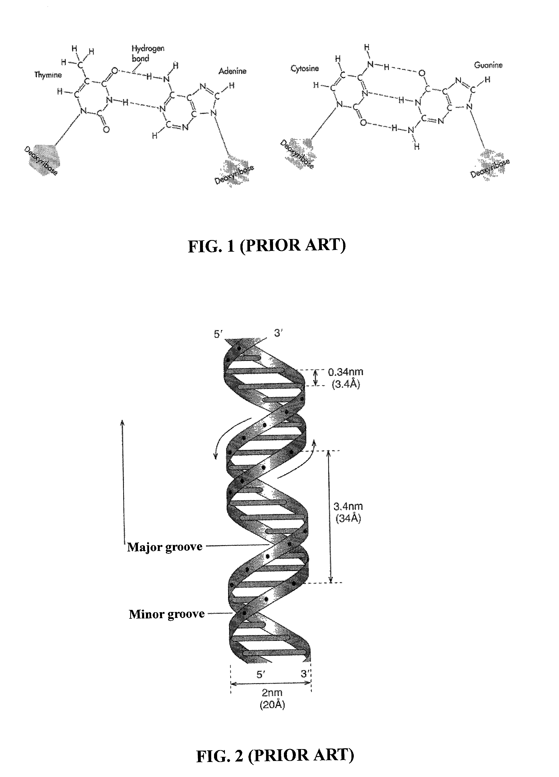
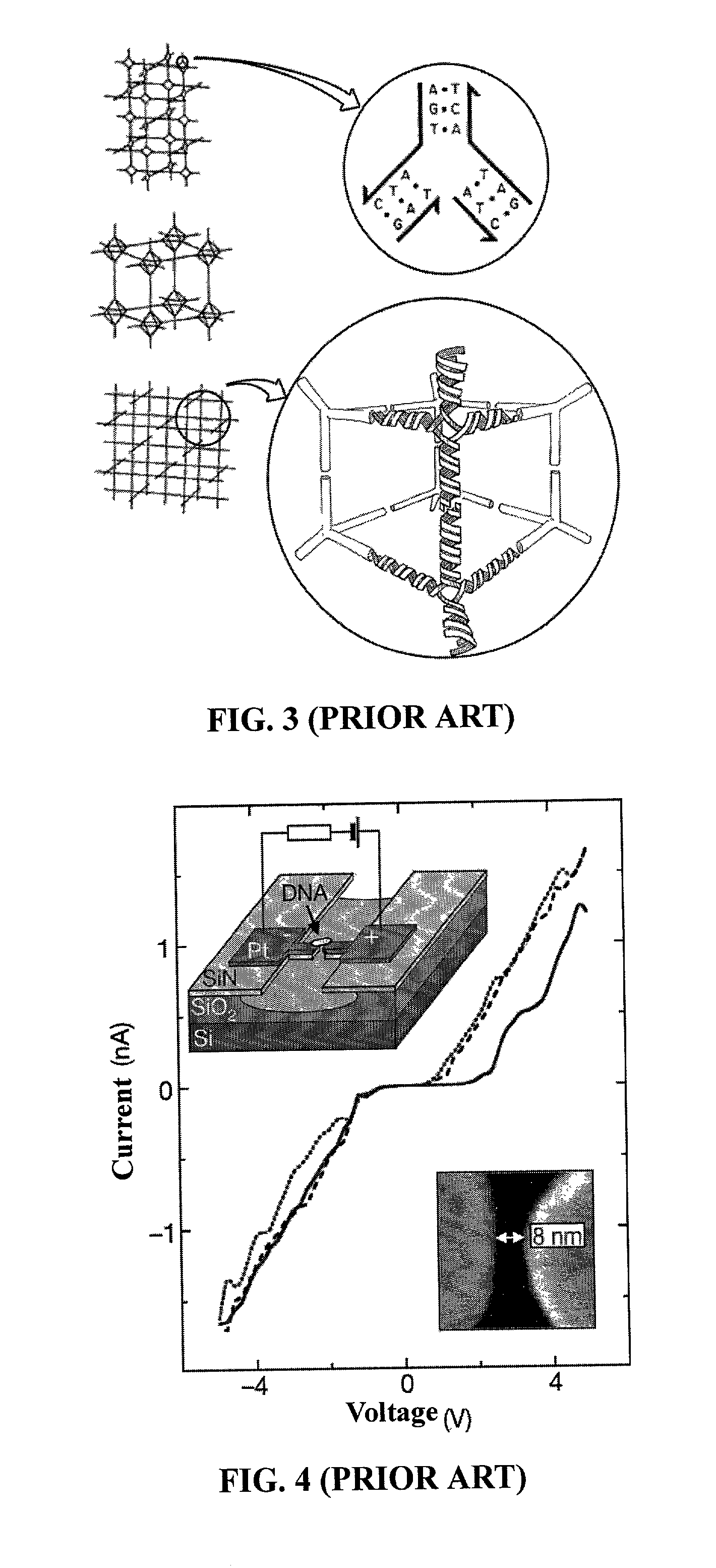
DNA-based integrated circuit
a technology of integrated circuits and dna, applied in the field of dna-based integrated circuits, can solve the problems of limiting photolithography technology, affecting circuit performance, and increasing the possibility of poor bonding
- Summary
- Abstract
- Description
- Claims
- Application Information
AI Technical Summary
Problems solved by technology
Method used
Image

Examples
example
[0032] Example of preparation and integration of DNA-based electronic elements
[0033] (1) Preparation of the DNA Sample
[0034] A. Purchasing DNA strings from Perkin Elmer (Taiwan) Co, Ltd; 21 G(21 bp), 19 cs(19 bp), 16 cs(19 bp), pBR322-S14(14 bp), pBR322-3A1 (1 7 bp), pBR322-5S1 (1 7 bp), pBR322-3A2(18 bp), pBR322-5S2(1 8 bp).
[0035] B. Producing Twin-DNA molecules through PCR.
[0036] Synthesize DNA with a commercial GeneAmp PCR Reagent Kit and a Ber Taq DNA polymerase Kit.
[0037] C. Alcohol Sedimentation (separate DNA with other impurities utilizing extremely low solubility of DNA saline in alcohol)
[0038] I . Add 10.about.20 .mu.L3.0 sodium acetate to 1 ml solution and mix it.
[0039] II. Add 1 ml alcohol (95%) and agitate, then place it in -20.degree. C. environment for 30.about.40 minutes.
[0040] III. In 4.degree. C. room temperature, centrifuge for 10 minutes at 13,000 rpm. Then wipe off upper liquid carefully.
[0041] IV. Add 0.5 ml alcohol to wash the DNA sediment, and then centrifuge ...
PUM
| Property | Measurement | Unit |
|---|---|---|
| diameter | aaaaa | aaaaa |
| distance | aaaaa | aaaaa |
| temperature | aaaaa | aaaaa |
Abstract
Description
Claims
Application Information