Organic EL device with high contrast ratio and method for maufacturing the same

a technology of organic el and contrast ratio, which is applied in the direction of identification means, instruments, discharge tubes, etc., can solve the problem of low contrast of devices having such a configuration

Inactive Publication Date: 2002-04-18
SAMSUNG DISPLAY CO LTD
View PDF3 Cites 17 Cited by
  • Summary
  • Abstract
  • Description
  • Claims
  • Application Information

AI Technical Summary

Problems solved by technology

However, the organic EL device having such a configuration has a problem of low contrast, because ambient light is reflected from the second electrode 15 made of a metal.

Method used


Image

  • Organic EL device with high contrast ratio and method for maufacturing the same
  • Organic EL device with high contrast ratio and method for maufacturing the same
  • Organic EL device with high contrast ratio and method for maufacturing the same

Examples


Embodiment Construction

[0023] A preferred embodiment of the present invention will be described in more detail, referring to the accompanying drawings.

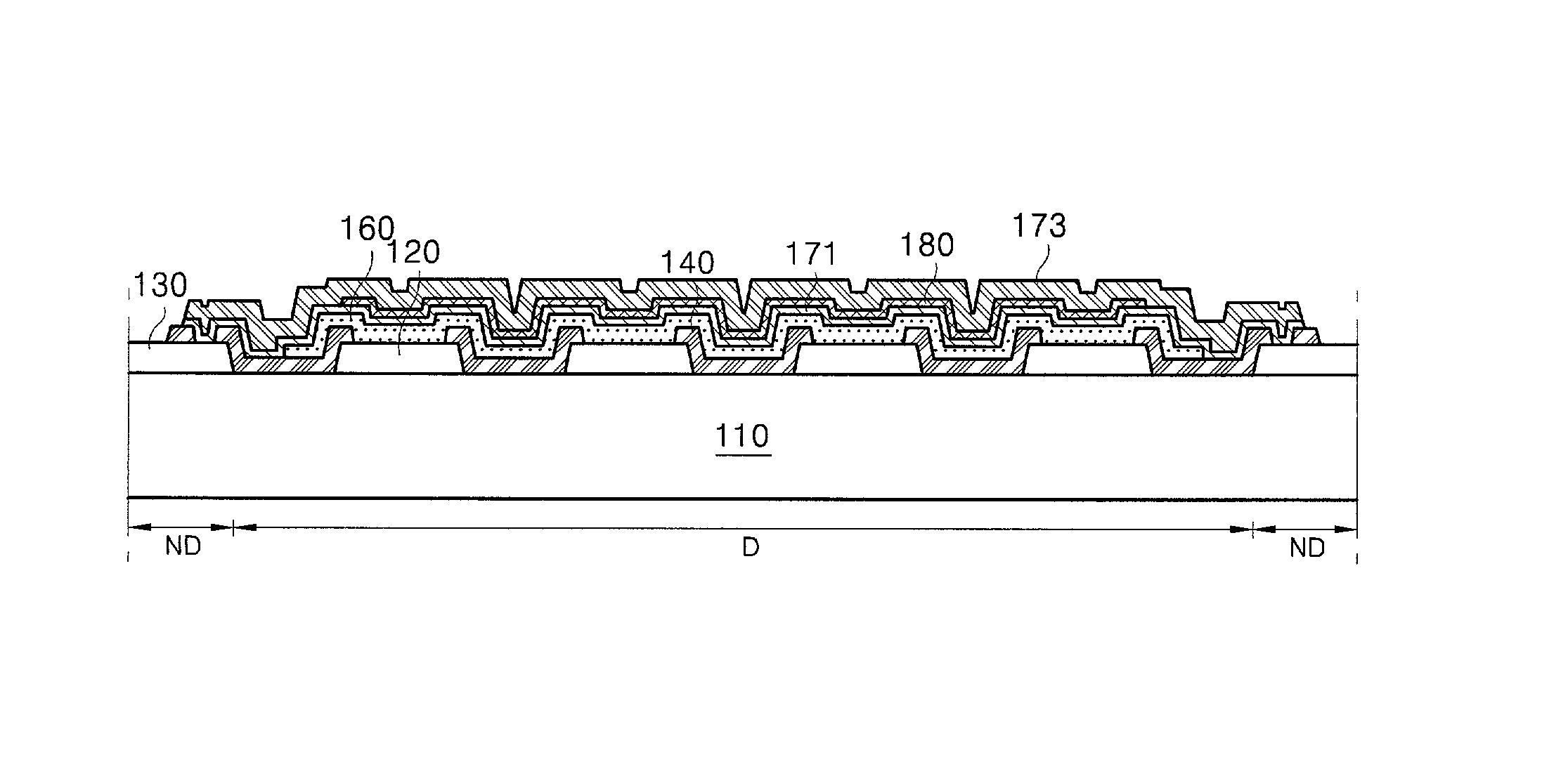
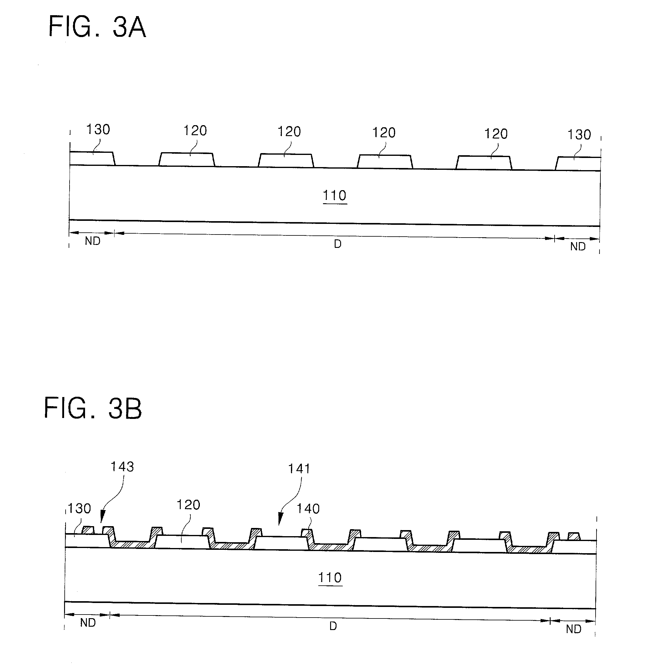
[0024] FIG. 3F is a cross-sectional view illustrating a passive matrix organic EL device according to the preferred embodiment of the present invention. As shown in FIG. 3F, a plurality of stripe-like shaped anode electrodes 120 are formed on a transparent substrate 110 spaced apart from each other at a predetermined interval. At this point, the transparent substrate 110 includes a display region D and a non-display region ND, and the display region D has a plurality of pixel region 141 (see FIG. 3B). Cathode leads 130 are formed on the non-display region ND in a perpendicular direction to the anode electrode 120. Interlayer insulators 140 cover the entire display region D except for the pixel region 141 and overlap an end portion of the cathode lead 130. The interlayer insulator 140 serves to insulate the adjacent two anode electrodes 120 and to define the...


PUM


Abstract

The present invention discloses an organic EL device, including: a transparent substrate having a display region and a non-display region, the display region having a pixel region; first electrodes formed on the display region of the substrate and spaced apart from each other; EL light-emitting layers formed on the portions of the first electrode corresponding to the pixel region; and second electrodes formed over the display region and having a light absorbing layer interposed therein.

Description

[0001] 1. Field of the Invention[0002] The present invention relates to an organic EL Device and a method for manufacturing the same.[0003] 2. Description of Related Art[0004] FIG. 1 is a cross-sectional view illustrating a conventional organic EL device. As shown in FIG. 1, the organic EL device includes a first electrode or anode electrode 13 formed on a substrate 11 and a second electrode or cathode electrode 15 with an EL light-emitting layer 17 interposed therebetween.[0005] A method for manufacturing such an organic EL device is as follows. First, an indium-tin oxide (ITO) film is formed all over a front surface of a glass substrate in a vacuum atmosphere. Then, the ITO film is formed into a stripe-like shape by etching, forming a plurality of transparent electrodes or first electrodes 13 arranged side by side but spaced apart from each other at predetermined intervals. Then, the EL light-emitting layer 17 is formed on the first electrode 13. The EL light-emitting layer 17 inc...

Claims


Application Information

Patent Timeline
Patent Type & Authority Applications(United States)
IPC IPC(8): G09F9/30H01L27/32H01L31/12H01L51/50H05B33/22H01L51/52H05B33/06H05B33/10H05B33/12H05B33/26
CPCH01L27/3283H01L51/5284H01L51/5221H10K59/173H10K50/826H10K50/865H01L31/12H05B33/26
Inventor CHO, SUNG-WOO
Owner SAMSUNG DISPLAY CO LTD
Why Eureka
Try Eureka