Semiconductor integrated circuit with resistor and method for fabricating thereof

Inactive Publication Date: 2002-05-23
SAMSUNG ELECTRONICS CO LTD
View PDF0 Cites 21 Cited by
  • Summary
  • Abstract
  • Description
  • Claims
  • Application Information

AI Technical Summary

Problems solved by technology

This variation in the resistance value of the self-alignment contact plug resistor causes a certain property of a semiconductor device provided with the resistor to be unstable.
Consequently it i

Method used


Image

  • Semiconductor integrated circuit with resistor and method for fabricating thereof
  • Semiconductor integrated circuit with resistor and method for fabricating thereof
  • Semiconductor integrated circuit with resistor and method for fabricating thereof

Examples


first embodiment

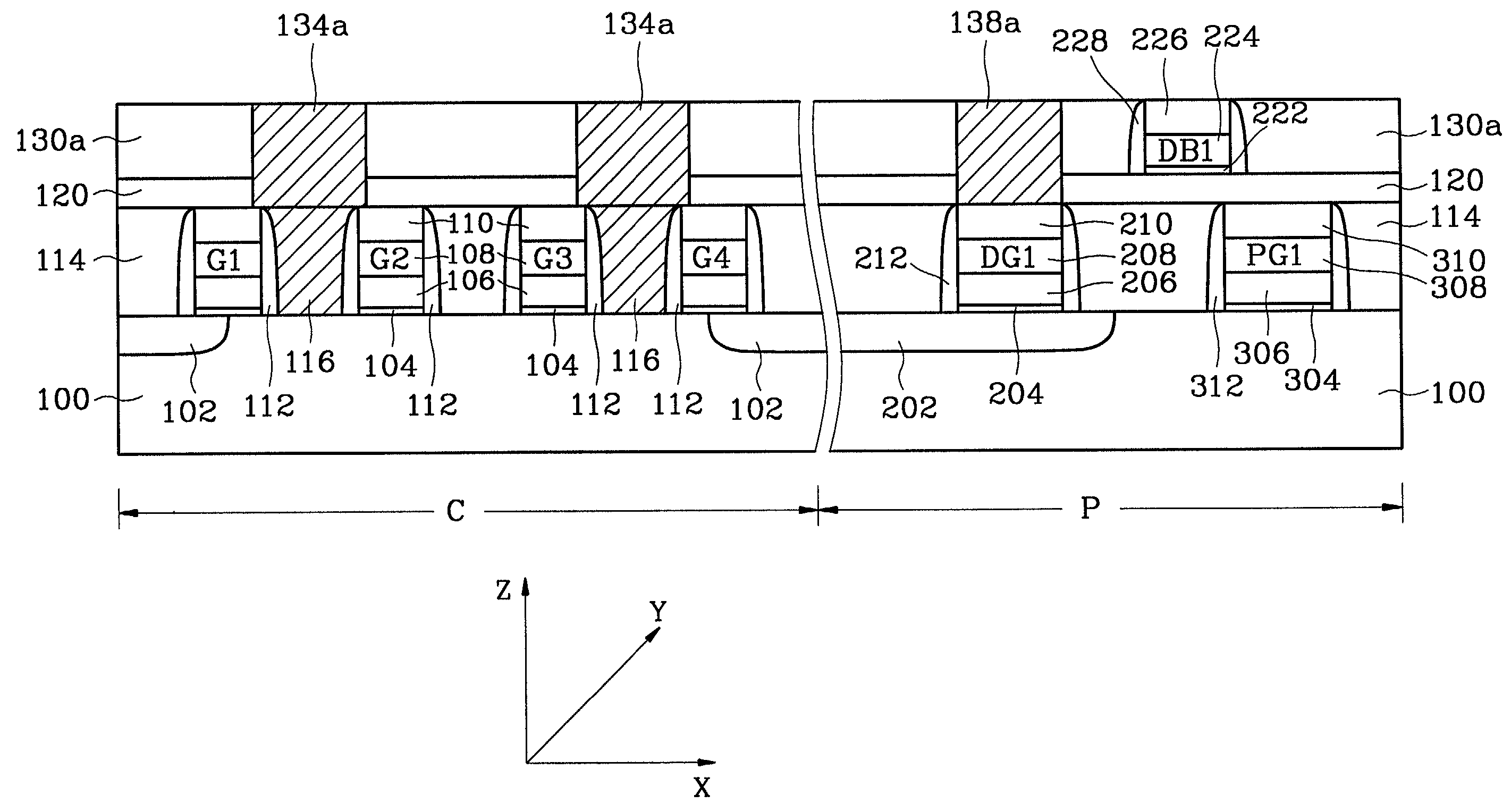
[0024] FIG. 1 is a cross sectional view illustrating a semiconductor integrated circuit provided with a resistor which is formed according to the present invention.

[0025] In this figure, a semiconductor substrate 100 is divided into two regions including a cell array region (C) and a peripheral circuit region (P). In the cell array region (C), a plurality of gate electrode structures G1, G2, G3, and G4 are formed on the semiconductor substrate of an active region limited by a device separating layer 102. Each of the gate electrode structures G1, G2, G3, and G4 includes a gate insulating layer 104, a polysilicon layer 106, a metal silicide layer 108, a gate electrode capping layer 110, and gate electrode spacers 112. In addition, storage electrode connection pads 116 which connect capacitors formed on each of the gate electrode structures to the active region on the semiconductor substrate 100, are formed between a first gate electrode structure GI and a second gate electrode structu...

second embodiment

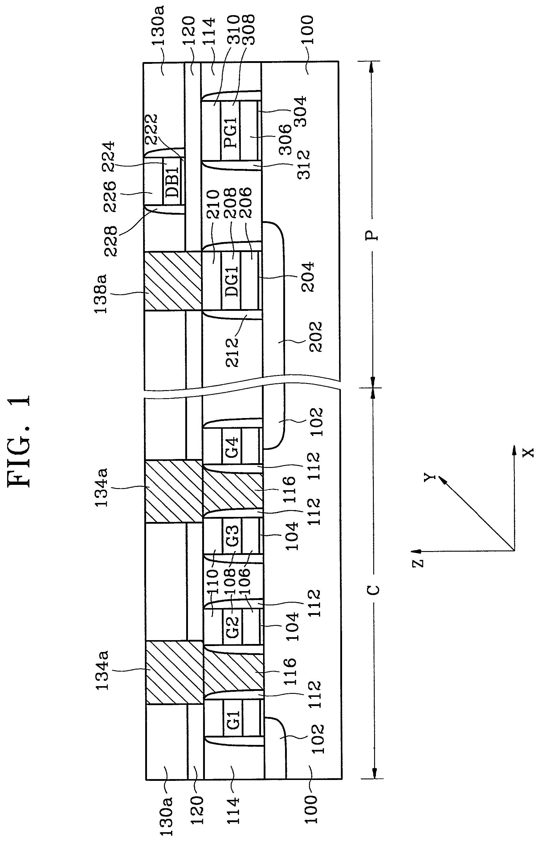
[0029] FIG. 2 is a cross sectional view illustrating a semiconductor integrated circuit provided with a resistor which is formed according to the present invention.

[0030] The semiconductor integrated circuit illustrated in this figure, is similar to that of FIG. 1 in the structure and components. For example, gate electrode structures G5, G6, G7, and G8 formed on a semiconductor substrate 400 in a cell array region (C), a storage electrode connection pad 416 in a first interlayer insulating layer 414, a bit line (not shown) which is arranged in a Y direction and is extended in a X direction, a bit line connection pad (not shown) formed in the first interlayer insulating layer 414, a storage electrode connection plug 432 within the second and third interlayer insulating layers, and a bit line structure connection plug (not shown) formed within the second interlayer insulating layer 420 are identical to those of the first embodiment, respectively. In this figure, reference numerals 40...

third embodiment

[0033] FIG. 3 is a cross sectional view illustrating a resistor used in a semiconductor integrated circuit according to the present invention.

[0034] The semiconductor integrated circuit illustrated in this figure, is similar to those of FIGS. 1 and 2 in the structure and components. For example, gate electrode structures G9, G10, G11, and G12 formed on a semiconductor substrate 600 in a cell array region (C), a storage electrode connection pad 616 in a first interlayer insulating layer 614, a bit line (not shown) which is arranged in a Y direction and is extended in a X direction, a bit line connection pad (not shown) formed in the first interlayer insulating layer 614, a storage electrode connection plug 632 within the second and third interlayer insulating layers 620 and 630A, and a bit line structure connection plug (not shown) formed within the second interlayer insulating layer 620 are identical to those of the first and second embodiments, respectively. In this figure, referen...


PUM


Abstract

A resistor which have a stable resistance value and a method for fabricating the same without increasing the area of a semiconductor integrated circuit. To prevent a dishing phenomenon, the resistor is formed on the dummy gate electrode structure which have been formed in a peripheral circuit region and/or it is formed between a pair of dummy bit line structures. Regardless of a process condition the width and height of the resistor can be determined in a certain range with use of the capping layer and spacers of the dummy gate electrode structure and/or the capping layer and/or spacers of the dummy bit line structure.

Description

[0001] 1. Field of the Invention[0002] The present invention relates to a semiconductor integrated circuit, and more particularly, to a semiconductor integrated circuit with a resistor and a method for fabricating thereof.[0003] 2. Description of the Related Art[0004] A semiconductor integrated circuit includes a cell array region consisting of a plurality of unit cells and a peripheral circuit region which is located in the outside of the cell array region and consists of semiconductor circuits which control operations and input / output of the unit cell, for example a driver, a buffer or an amplifier. Each of the semiconductor circuits used in the two regions includes a transistor which is an active device and a resistance which is a passive device, basically. Consequently, a manufacturing process of a semiconductor integrated circuit accompanies processes of forming a plurality of transistors and resistors. In addition when a semiconductor device is formed in a cell array region, a...

Claims


Application Information

Patent Timeline
IPC IPC(8): H01L21/02H01L27/06H01L27/02
CPCH01L28/20H01L27/0688H01L27/02
Inventor SHIN, SOO-HOYANG, WON-SUK
Owner SAMSUNG ELECTRONICS CO LTD
Why Eureka
Try Eureka