Display apparatus and driving method thereof

a technology of display apparatus and driving method, which is applied in the direction of static indicating device, non-linear optics, instruments, etc., can solve the problems of short interval between battery charging of mobile instruments, increase in cost, and complicated driving circuit structur

Inactive Publication Date: 2002-06-20
JAPAN DISPLAY CENTRAL CO LTD
View PDF4 Cites 93 Cited by
  • Summary
  • Abstract
  • Description
  • Claims
  • Application Information

AI Technical Summary

Problems solved by technology

Since power consumption in the color display device is larger than that in the monochrome display device, the color display device has a problem that an interval of battery charging of the mobile instrument is short.
Furthermore, since a circuit is also complicated, miniaturization is difficult, which leads to increase in cost.
In case of the color display device, however, not only the structure of the driving circuit is complicated, but a capacity of a memory storing therein pixel data is also increased.
Therefore, it is technically difficult to integrally form the driving circuit on the pixel array substrate.
In such control in accordance with each horizontal pixel line, however, the low-consumption power is not necessarily attained as compared with control at the time of usual driving.
Moreover, as a realistic problem, the memory corresponding to only one pixel is rarely rewritten.
Since the memories corresponding to several tens pixels are typically collectively rewritten, even if the memories are rewritten in accordance with each block, this does not necessarily lead to the redundant operation such that the consumption power is wasted.
However, since burning and the like of the liquid crystal occurs when a direct-current voltage is applied to the liquid crystal for a long period, the polarity inversion operation must be carried out at predetermined intervals even in the standby mode.

Method used


Image

  • Display apparatus and driving method thereof
  • Display apparatus and driving method thereof
  • Display apparatus and driving method thereof

Examples


specific example 2

of Memory and Polarity Inverting circuit

[0080] FIG. 7 is a circuit diagram of a double-word line structure. The circuit shown in FIG. 7 has a transistor Q6 which is turned on / off by the potential of a row word line. When the transistor Q6 is turned on, the potential of the main word line is supplied to the sub word line. The sub word line is connected to each of the sub pixels aligned in the row direction. For example, when the sub word line is on the high level, a transistor Q3 is turned on, and a transistor Q7 provided in a feedback path of the SRAM is turned off. At this moment, either the transistor Q4 or Q5 is turned on by the potential of the polarity control lines P+ and P-.

[0081] On the other hand, when the sub word line is on the low level, the transistor Q7 is turned on, and an inverter output on the rear stage side in the SRAM is fed back to the input of the inverter on the first stage side, thereby holding data.

[0082] As described above, in the double word line structure...

specific example 3

of Memory and Polarity Inverting circuit

[0084] FIG. 9A is a circuit diagram showing an example in which the data line and the polarity control lines P+ and P- are shared by adjacent pixels. The circuit shown in FIGS. 9A-9B are an example that four weighted sub pixels composes one pixel and 16-gradation display is realized by each pixel. Four sub pixels are arranged so that each two sub pixels are provided in the both vertical and horizontal directions, and two sub pixels adjacent to each other in the horizontal direction are arranged through the data line and share this data line. The sub pixel has a transistor Q3 connected to the data line, an SRAM and a polarity inverting circuit. The SRAM has transistors Q4 and Q5 and inverters IV3 and IV4, and the polarity inverting circuit has transistors Q4 and Q5.

[0085] In the circuit shown in FIGS. 9A-9B, since the sub pixels 100 adjacent to each other in the horizontal direction share the data line, separate word lines must be connected to ...

first embodiment

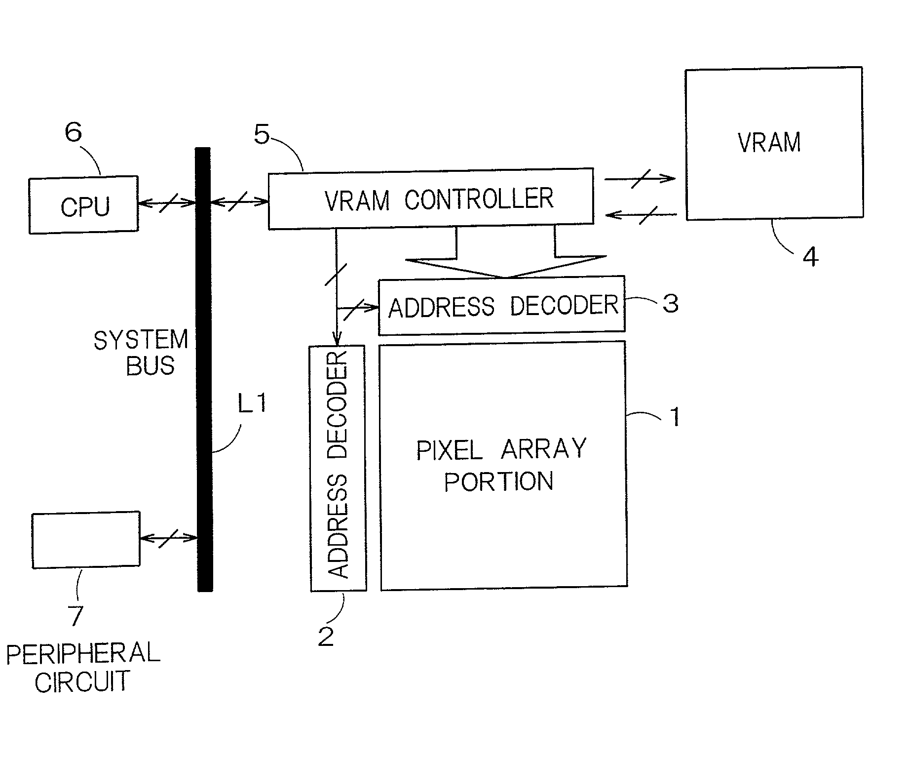
[0112] A preferred specific example of the liquid crystal display will now be described with reference to FIG. 1.

[0113] This liquid crystal display is of a light reflex type in the four-inch diagonal size used for PDA, which includes a display area of a total pixel number 320 (.times.3).times.480.

[0114] FIG. 21 is a view of this liquid crystal display, FIG. 22 is a view showing schematic configuration of the display area, and FIG. 23 is a partially schematic cross-sectional view of the liquid crystal display.

[0115] This liquid crystal display is formed on an array substrate 200 formed of e.g. a glass, as an insulating substrate. A display array portion 1, a pair of Y address decoders 2a and 2b, an X address decoder 3 and an interface portion 5a including a part of functions of the VRAM controller 5 depicted in FIG. 1 are integrally formed by, e.g., a polycrystalline silicon transistor (p--Si TFT) on the array substrate 200.

[0116] When the above-described interface portion 5a is int...


PUM

PropertyMeasurementUnit
threshold voltageaaaaaaaaaa
voltagesaaaaaaaaaa
ground voltage VSSaaaaaaaaaa

Abstract

A liquid crystal display device which can reduce power consumption and can be miniaturized. The liquid crystal display device according to the present invention includes a pixel array portion, an address decoder, a display memory (VRAM), and a VRAM controller, and transmits / receives a signal to / from a CPU and a peripheral circuit through a system bus. The pixel array portion has an area gradation pixel structure in which each pixel is composed of a plurality of one-bit memories. The entire pixel array portion is divided into pixel blocks each of which consists of a plurality of pixels, and the one-bit memory is rewritten in units of block. The one-bit memory has a double-word line structure.

Description

[0001] This application is based upon and claims the benefit of priority from the prior Japanese Patent Applications No. 2000-269177, filed on Sep. 5, 2000, the entire contents of which are incorporated herein by reference.[0002] 1. Field of the Invention[0003] The present invention relates to a display device, and more specifically, it relates to a technique for reducing power consumption and simplifying a circuit configuration.[0004] 2. Related Background Art[0005] Monochrome display devices were often provided in conventional mobile instruments such as mobile phones. Recently, with increase of opportunities such as connections to an Internet using the mobile instruments, the mobile instruments having color display devices has increased.[0006] Since power consumption in the color display device is larger than that in the monochrome display device, the color display device has a problem that an interval of battery charging of the mobile instrument is short. Furthermore, since a cir...

Claims


Application Information

Patent Timeline
Patent Type & Authority Applications(United States)
IPC IPC(8): G02F1/133G09G3/20G09G3/32G09G3/36
CPCG09G3/2022G09G3/2074G09G3/32G09G3/3614G09G3/3618G09G2330/021G09G2300/0452G09G2300/0828G09G2300/0842G09G2300/0857G09G3/3666G02F1/133
Inventor NAKAMURA, TAKASHI
Owner JAPAN DISPLAY CENTRAL CO LTD
Why Eureka
Try Eureka