Linear voltage controlled oscillator transconductor with gain compensation

a transconductors and voltage control technology, applied in the direction of pulse generators, pulse techniques, electrial characteristics varying frequency control, etc., can solve the problems affecting the stability and noise of the pll circuit, and achieve the effect of less gain, more gain, and decreased variable resistan

Inactive Publication Date: 2002-07-11
MARVELL ASIA PTE LTD
View PDF0 Cites 17 Cited by
  • Summary
  • Abstract
  • Description
  • Claims
  • Application Information

AI Technical Summary

Benefits of technology

0015] The voltage controlled oscillator includes a current controlled oscillator comprising a ring oscillator. The voltage signal having variable frequency is further comprised of a differential transistor output; the input voltage signal is comprised of a differential transistor pair. The digital control circuitry is adapted to output directly to the transconductor, and to adjust and control a center frequency of the current controlled oscillator. The digital control circuitry further comprises a digitally controlled variable resistance circu

Problems solved by technology

As noted, however, the gain of a VCO may also vary widely with process, and if left uncontrolled

Method used


Image

  • Linear voltage controlled oscillator transconductor with gain compensation
  • Linear voltage controlled oscillator transconductor with gain compensation
  • Linear voltage controlled oscillator transconductor with gain compensation

Examples


first embodiment

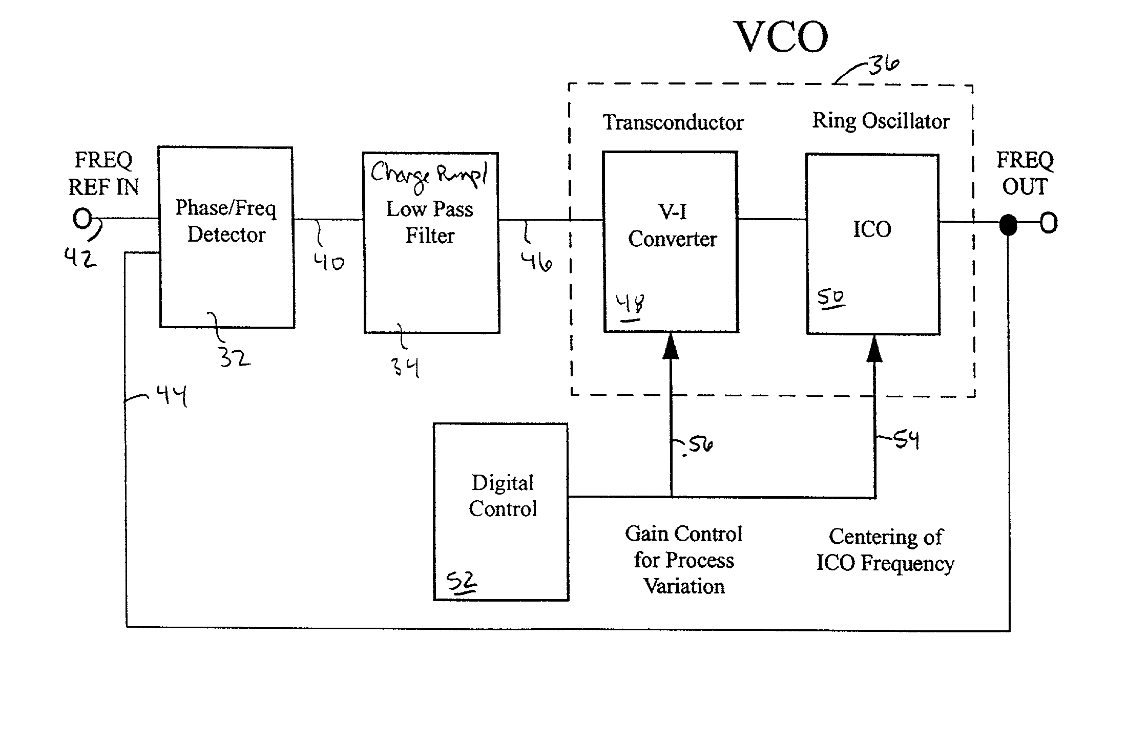
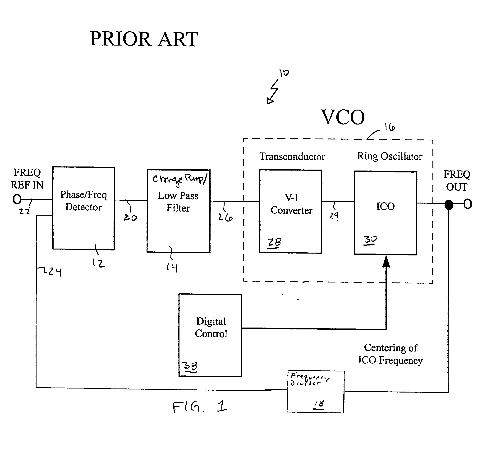
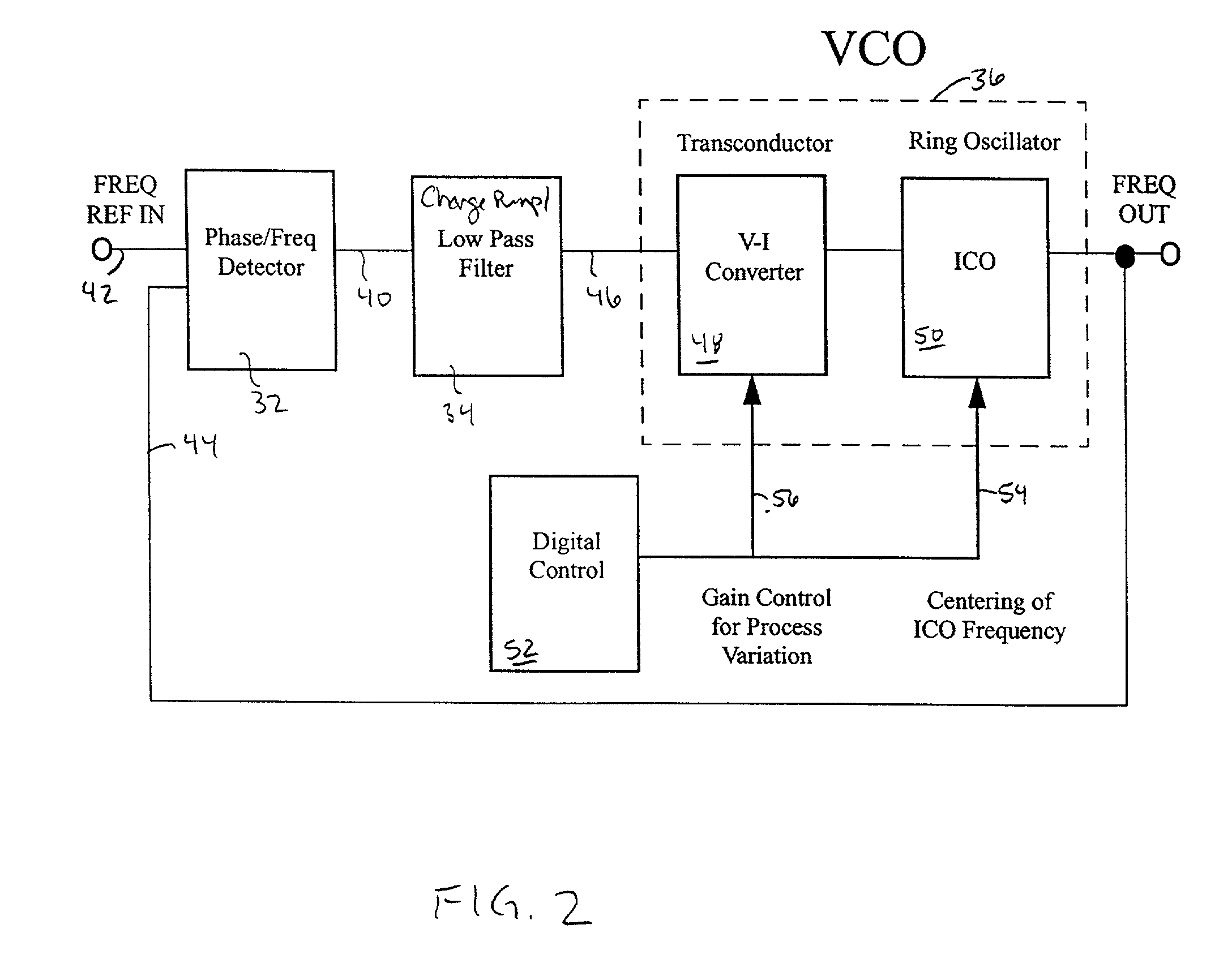
[0030] FIG. 3 represents the present invention, a digitally controlled variable resistance transconductor. In this embodiment, a digitally controlled variable resistance is used to regulate and control the transconductor gain. The differential voltage input from the low pass filter, V.sub.p 101 and V.sub.n 102, respectively, are received by an NFET differential pair 103, 104. Variable resistors 105, 106 are digitally controlled by a digital to analog converter (DAC) 110 having control lines CNTL0, CNTL1, CNTL2, CNTL3, and the like, corresponding to each bit activated by the DAC. The control lines increment the variable resistance of resistors 105, 106. By connecting the variable resistors to supply voltage V.sub.DD 107, source-coupled NFETS 103 and 104, and constant current source 108, a digitally controlled differential amplifier 109 is formed. NFETS 112 and 114 and current source 115 form a second differential amplifier which converts the voltages at 105 and 106 to currents throug...

second embodiment

[0035] Importantly, transistor mirror banks 308, 306 are controlled by the DAC control lines to allow for switching of the variable output lines of the mirror banks. Unlike the second embodiment, no voltage level shifting is necessitated in this embodiment. Transistor banks 312, 314, and 318 provide switches to turn on / off corresponding current carrying lines. Through selective digital switching of the transistors responsible for carrying the current, i.e., transistor banks 312, 314, and 318, various levels of current may be screened and selected.


PUM


Abstract

A voltage controlled oscillator of a phase locked loop circuit having digitally controlled gain compensation. The digital control circuitry provides binary logic input to the voltage controlled oscillator for a digitally controlled variable resistance circuit, a digitally controlled variable current transconductor circuit, or differential transistor pairs having mirrored circuitry for adjusting the V-I gain. The latter configuration requires the voltage controlled oscillator to incorporate a source-coupled differential pair which is driven by a low pass filter capacitor output voltage, and connected to load transistors; a current source and a current mirror for generating a tail current; individual banks of transistors to mirror the load transistor currents; a digital-to-analog converter with control lines outputted there from, the digital-to-analog converter used to increase the amount of current allowed to flow to the transconductor output, the current being digitally increased and decreased corresponding to an amount of current pulled from the current source, and mirroring the current through at least one transistor mirror circuit.

Description

[0001] 1. Field of the Invention[0002] The present invention relates generally to a phase locked loop (PLL) circuit, and more particularly, to a circuit for digitally controlling the voltage controlled oscillator (VCO) gain and minimizing variations in the gain due to manufacturing process tolerances.[0003] 2. Description of Related Art[0004] A phase locked loop circuit outputs a signal synchronized with an input signal. Essentially, it produces an output signal which tracks an input signal in frequency and exhibits a fixed phase relationship to the input signal. FIG. 1 depicts a conventional PLL circuit 10 which is generally comprised of a phase / frequency detector 12, a charge pump and low pass filter 14, a voltage controlled oscillator 16, and if necessary, a frequency divider 18. If the clock frequency input to the phase detector and the output frequency of the voltage controlled oscillator are equal, the frequency divider 18 is not required.[0005] The phase detector 12 is a devi...

Claims


Application Information

Patent Timeline
IPC IPC(8): H03B1/00H03L7/089H03L7/093H03L7/099
CPCH03B2201/0291H03L7/0891H03L7/093H03L7/0995
Inventor MULLGRAV, ALLAN L. JR.SORNA, MICHAEL A.
Owner MARVELL ASIA PTE LTD
Why Eureka
Try Eureka