Method and system for detecting metal contamination on a semiconductor wafer

a metal contamination and semiconductor wafer technology, applied in individual semiconductor device testing, semiconductor/solid-state device testing/measurement, instruments, etc., can solve the problems of metal contamination having a significant impact on the performance and reliability of semiconductor devices, degrading the electrical properties of semiconductor substrates, and affecting the performance of semiconductor devices

Inactive Publication Date: 2002-07-11
KLA TENCOR TECH CORP
View PDF0 Cites 59 Cited by
  • Summary
  • Abstract
  • Description
  • Claims
  • Application Information

AI Technical Summary

Problems solved by technology

Metal contamination on a semiconductor substrate may degrade the electrical properties of the semiconductor substrate.
When metal contamination is present in a dielectric material formed upon the semiconductor substrate or on a surface of the semiconductor substrate, the metal contamination may cause the electrical properties of the dielectric material to degrade.
Metal contamination may have a significant impact on the performance and reliability of semiconductor devices.
Metal contamination may be deposited on a semiconductor wafer during processing and manufacturing of semiconductor devices.
In many cases, a portion or substantially all of the metal contamination may be deposited on the surface of the semiconductor substrate due to problems in processing or improper handling of the semiconductor substrates.
The disadvantage to using one of these physical analysis techniques to determine the metal contamination is that these measurement techniques generally take a very long time.
In addition, SIMS and VPD-ICPMS are destructive techniques which generally require removal of a portion of the dielectric material or semiconductor substrate during the measurement process.
As such, device based electrical characterization may be expensive and time consuming.
In addition, analyzing the data also becomes complicated due to the number of processing steps that may be performed in order to form the semiconductor devices on the dielectric material or on the semiconductor substrate.
Furthermore, the metal contamination may include metal contamination in a portion of the dielectric material.
As such the annealing process may cause degradation of the dielectric material.
In this manner, the extent to which the metal contamination may be driven into the dielectric material by the annealing process may be limited by an acceptable amount of degradation in the dielectric material which may be caused by the annealing process.
The period of time for which the semiconductor substrate may be ...

Method used


Image

  • Method and system for detecting metal contamination on a semiconductor wafer
  • Method and system for detecting metal contamination on a semiconductor wafer
  • Method and system for detecting metal contamination on a semiconductor wafer

Examples


Embodiment Construction

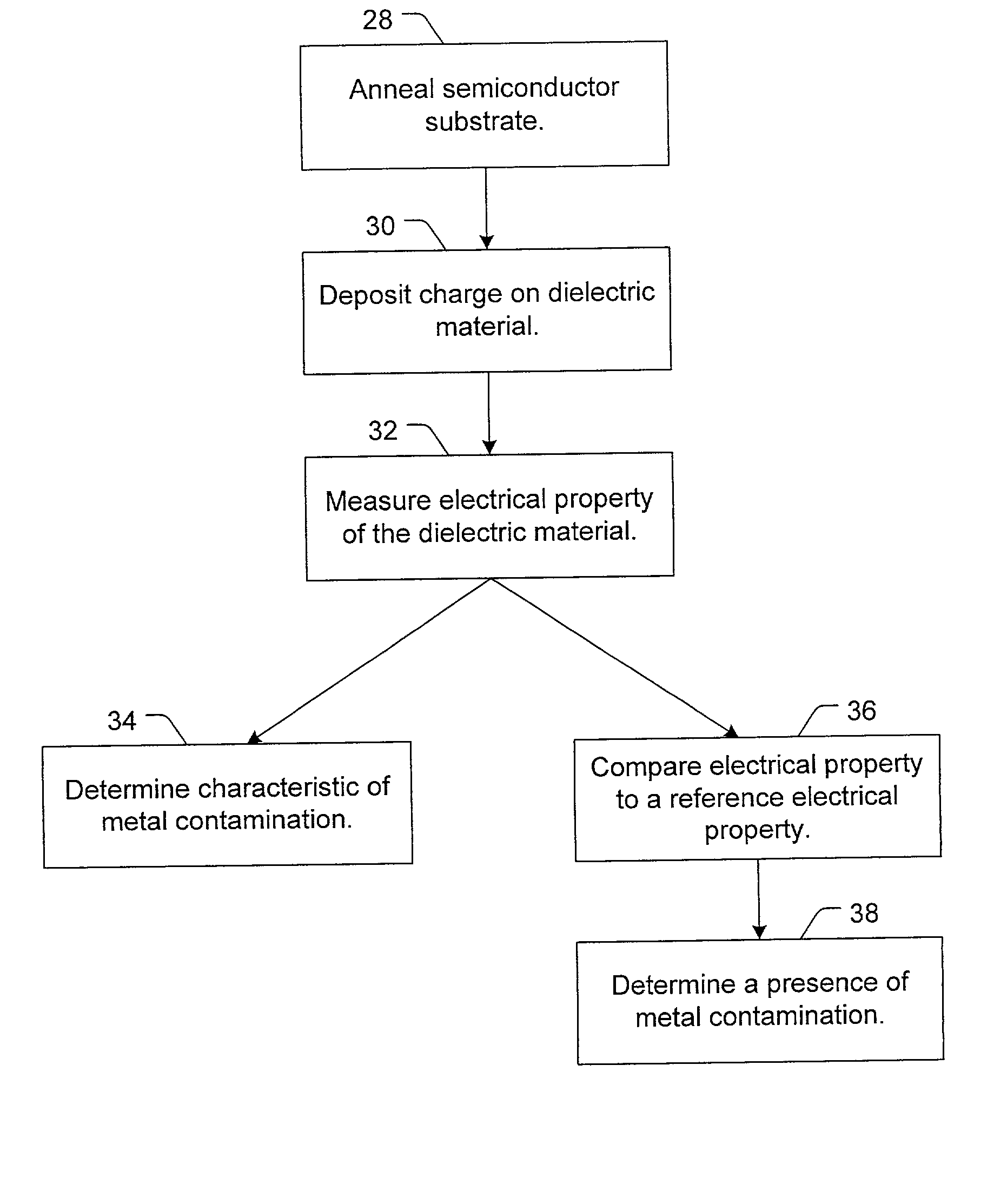
[0081] Effect of an Annealing Process on Detection of Metal Contamination.

[0082] A silicon dioxide dielectric material was formed on a silicon substrate. An annealing process was performed at various temperatures to drive copper metal contamination into the dielectric material. The temperatures included 20.degree. C., 300.degree. C., and 450.degree. C. A control wafer was also measured after an annealing process, which included heating the semiconductor substrate at 450.degree. C. The control wafer was a silicon dioxide dielectric material formed on a silicon semiconductor substrate which was substantially free of copper metal contamination. A charge was deposited on an upper surface of each dielectric material. The tunneling voltage of the dielectric material was measured at various positions on the semiconductor substrate. In addition, the tunneling field was determined as a function of the tunneling voltage at each measurement position. FIG. 6 illustrates a plot of the tunneling ...


PUM


Abstract

A method to detect metal contamination on a semiconductor topography is provided. The semiconductor topography may include a semiconductor substrate or a dielectric material disposed upon a semiconductor substrate. The metal contamination may be driven into the semiconductor substrate by an annealing process. Alternatively, the annealing process may drive the metal contamination into the dielectric material. Subsequent to the annealing process, a charge may be deposited upon an upper surface of the semiconductor topography. An electrical property of the semiconductor topography may be measured. A characteristic of at least one type of metal contamination may be determined as a function of the electrical property of the semiconductor topography. The method may be used to determine a characteristic of one or more types of metal contamination on a portion of the semiconductor topography or the entire semiconductor topography. A system configured to detect metal contamination on a semiconductor topography is also provided. An oven may be incorporated into the system and may be used to anneal the semiconductor topography. The system may also include a device that may be configured to deposit a charge on an upper surface of the semiconductor topography. A sensor may also be included in the system. The sensor may use a non-contact work function technique to measure an electrical property of the semiconductor topography.

Description

PRIORITY CLAIM[0001] This application claims priority to U.S. Provisional Application No. 60 / 203,538 entitled "Method and System for Detecting Metal Contamination on a Semiconductor Wafer," filed May 10, 2000.[0002] 1. Field of the Invention[0003] This invention generally relates to detecting metal contamination. Certain embodiments relate to determining metal contamination in a semiconductor substrate or a dielectric material by measuring electrical parameters of the semiconductor substrate or the dielectric material.[0004] 2. Description of the Related Art[0005] Metal contamination on a semiconductor substrate may degrade the electrical properties of the semiconductor substrate. For example, metal contamination in the bulk semiconductor substrate may cause the bulk minority carrier lifetime to decrease because the metal contamination may assist in the recombination of electrons and holes in the semiconductor substrate. When metal contamination is present in a dielectric material f...

Claims


Application Information

Patent Timeline
IPC IPC(8): G01N27/00G01N27/60H01L21/66
CPCG01N27/002G01N27/60H01L22/12H01L2924/0002H01L2924/00
Inventor XU, ZHIWEISRIVATSA, ARUNSAMSAVAR, AMINMILLER, THOMAS G.HORNER, GREGWEINZIERL, STEVEN
Owner KLA TENCOR TECH CORP
Why Eureka
Try Eureka