Methods Of Attaching A Sheet Of An Adhesive Film To A Substrate In The Course Of Making Integrated Circuit Packages

a technology of adhesive film and integrated circuit, which is applied in the field of integrated circuit packaging, can solve the problems of a relatively large amount of time spent on the step, and achieve the effects of reducing inventory and labor costs, improving the quality of lamination between the adhesive film and the substrate, and increasing efficiency

Inactive Publication Date: 2002-07-25
AMKOR TECH INC
View PDF0 Cites 9 Cited by
  • Summary
  • Abstract
  • Description
  • Claims
  • Application Information

AI Technical Summary

Benefits of technology

[0012] The methods of the present invention greatly improve on prior art processes that attach a discrete adhesive film sheet to each package site of the substrate strip. In the prior art, the adhesive films are each sized for one and only one package site, and are individually placed and cured. The processes of the present invention are much faster than such processes, since a larger sheet of adhesive film is placed on the substrate. Typically, the substrate strip will have a plurality of rows and columns of package sites and, in one embodiment of the present invention, a continuous sheet of adhesive film is applied to the substrate strip so as to cover all of the rows and columns of package sites with the continuous sheet of adhesive film. Using a single large sheet of adhesive film, rather than many smaller single-package-size adhesive film sheets, provides a remarkable gain in efficiency. Moreover, inventory and labor costs are reduced because different sizes and shapes of adhesive films do not have to be used or kept in inventory. Finally, the quality of the lamination between the adhesive film and the substrate is improved. In one embodiment, this improved lamination is achieved by running the substrate strip and the adhesive film under a roller that applies pressure and / or heat uniformly across a plurality of package sites.

Problems solved by technology

First, the step takes a relatively large amount of time because adhesive films 14 are placed and cured one at a time.

Method used


Image

  • Methods Of Attaching A Sheet Of An Adhesive Film To A Substrate In The Course Of Making Integrated Circuit Packages
  • Methods Of Attaching A Sheet Of An Adhesive Film To A Substrate In The Course Of Making Integrated Circuit Packages
  • Methods Of Attaching A Sheet Of An Adhesive Film To A Substrate In The Course Of Making Integrated Circuit Packages

Examples


Embodiment Construction

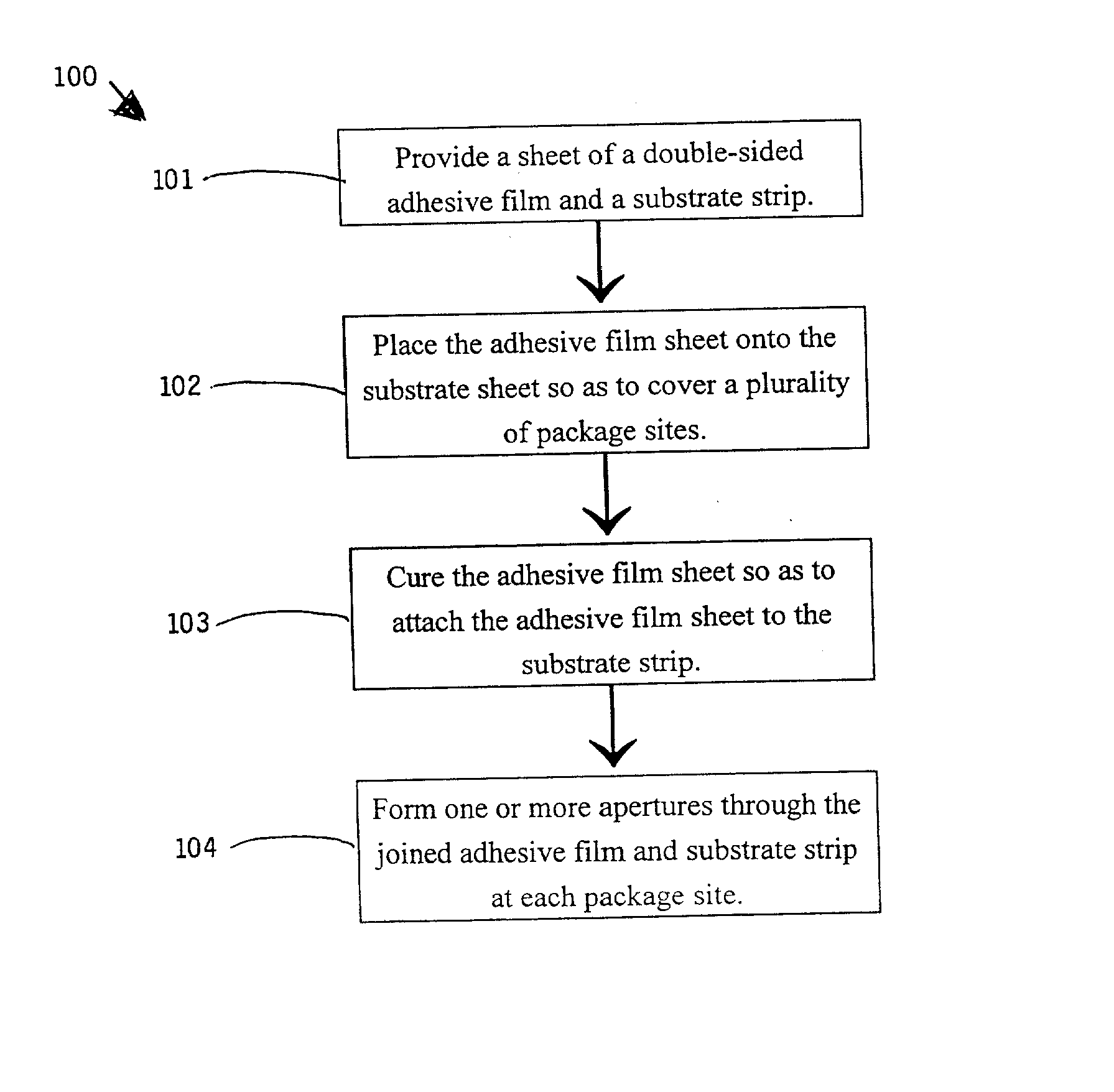
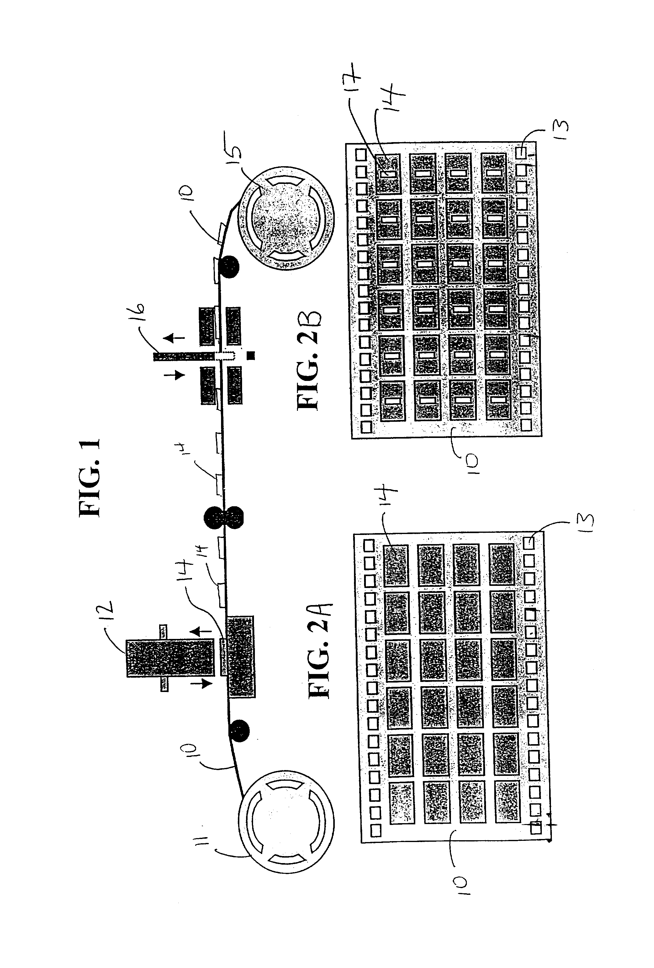
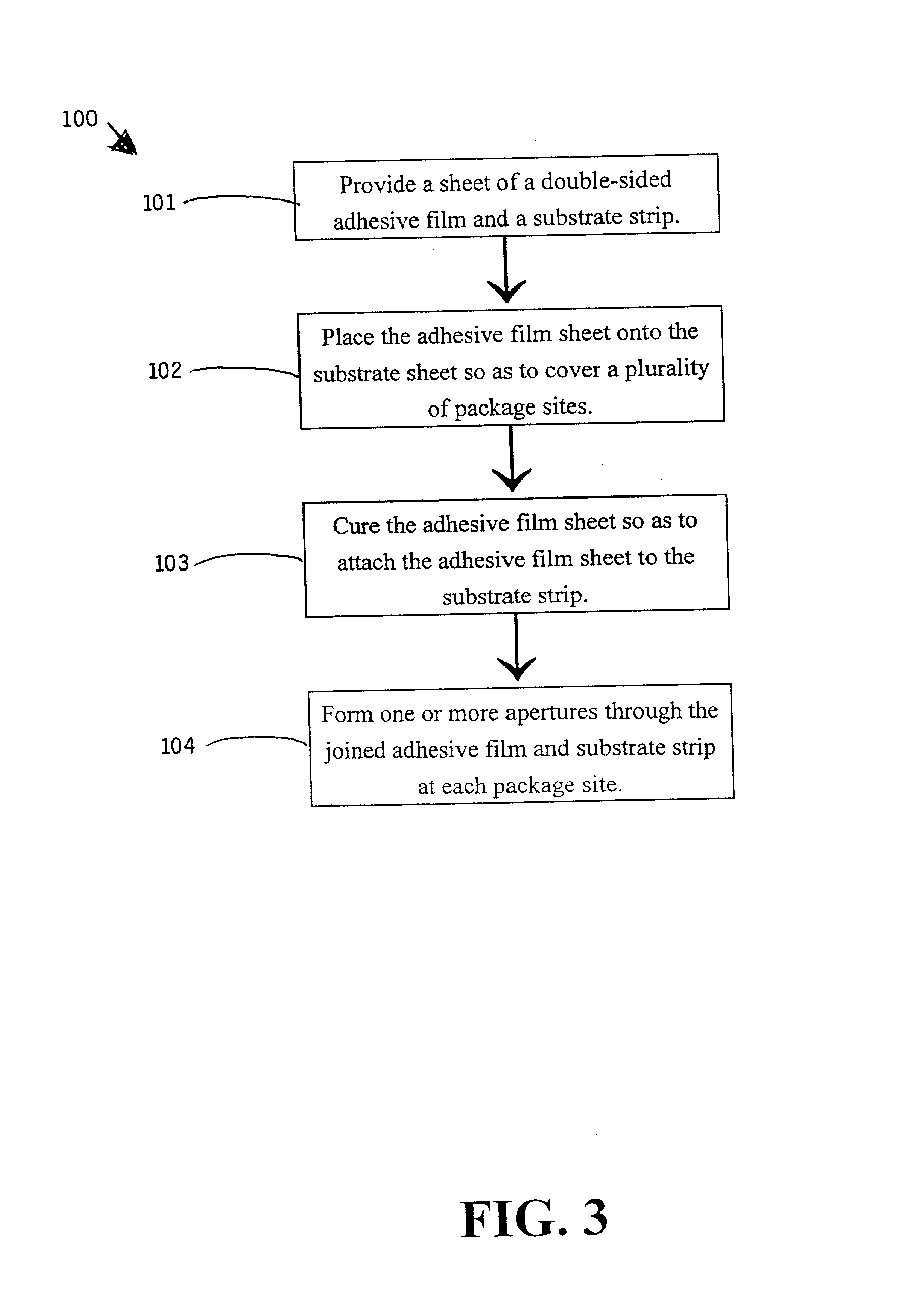
[0025] FIG. 3 is a flow chart of an embodiment of a method 100 within the present invention for applying a sheet of an adhesive film to a substrate strip and forming apertures in the joined adhesive film sheet and substrate strip at package sites where individual packages are to be fabricated. FIG. 4 is a side view of a sheet 30 of an adhesive film being attached to a substrate strip 10 and then punched with a punch 16 to form apertures 17. FIG. 5A is a plan view of a substrate strip 10 after a large, continuous adhesive film sheet 30 is attached to substrate strip 10 according to one embodiment of the present invention. FIG. 5B is a plan view of apertures 17 formed in substrate strip 10 and adhesive film sheet 30.

[0026] Step 101 of method 100 of FIG. 3 provides a sheet 30 of a double-sided adhesive film. Referring to FIGs. 4 and 5A, adhesive film sheet 30 typically will be provided on a roll 34. Adhesive film sheet 30 has a first surface 31 and an opposite second surface 32. Dispos...


PUM

PropertyMeasurementUnit
thicknessaaaaaaaaaa
temperatureaaaaaaaaaa
pressureaaaaaaaaaa

Abstract

<heading lvl="0">Abstract< / heading> Methods of making packages for integrated circuit devices are described. An exemplary method includes providing a substrate sheet having an array of package sites at which individual integrated circuit packages will be assembled. A continuous sheet of an adhesive film is placed on the substrate strip so as to cover the plurality of package sites. The adhesive film sheet is then cured by applying heat or pressure or heat and pressure to the substrate strip and the sheet of adhesive film. The pressure and / or heat cause the sheet of adhesive film to be permanently attached to the substrate strip. A subsequent step forms one or more apertures though the joined substrate strip and adhesive film at each package site. An integrated circuit die is mounted on the adhesive film at each package site, and bond wires are attached through the aperture between metallizations of the substrate and the integrated circuit device. After the one or more apertures at each site are filled with an insulative material, the adjacent package sites are separated, forming individual packages each having an integrated circuit device.

Description

Background of Invention[0001] 1.Field of the Invention The present invention concerns packaging for integrated circuits, and in particular concerns a method for attaching a sheet of an adhesive film to a substrate used to manufacture a plurality of integrated circuit packages.[0002] 2.Description of Related Art Integrated circuit packages typically include an integrated circuit die attached to a substrate by an adhesive layer. Bond wires or equivalent conductors are connected between the integrated circuit die and metallizations on the substrate. The metallizations are connected to other metal structures of the substrate, such as bonding pads or solder balls, for connecting the package to a printed circuit board.[0003] Typically, a plurality of packages are built in parallel on substrate strip. The strip may be formed, for example, of a thin insulative film such as a polyimide film or an epoxy laminate film. Alternatively, the substrate strip may be an array of interconnected metal ...

Claims


Application Information

Patent Timeline
Patent Type & Authority Applications(United States)
IPC IPC(8): H01L21/56H01L23/31
CPCH01L2224/48091H01L2924/00014H01L2224/97H01L2224/83H01L2224/92147H01L2224/73215H01L2924/15311H01L21/56H01L21/561H01L23/3114H01L24/97H01L2224/4824H01L2924/01027H01L2924/01074H01L2924/14H01L2224/85H01L24/48H01L2924/01005H01L2924/01006H01L2924/01033H01L2224/32225H01L2924/00Y10T156/1089Y10T156/1092Y10T29/53178H01L2224/05554H01L2224/05599H01L2224/45099H01L2224/85399H01L2924/181H01L2924/00012H01L2224/45015H01L2924/207
Inventor SHIM , IL KWONCHUN , DO SUNGDICAPRIO , VINCENTHOFFMAN , PAUL
Owner AMKOR TECH INC
Why Eureka
Try Eureka