Shift register having fewer lines therein, and liquid crystal display having the same

a shift register and fewer lines technology, applied in the field of shift registers, can solve the problems of increasing the number of lines in the shift register and the increase in achieve the effect of reducing the area required for wiring, reducing the influence of display capabilities, and reducing the size of the wiring area

Inactive Publication Date: 2002-07-25
MIND FUSION LLC
View PDF0 Cites 34 Cited by
  • Summary
  • Abstract
  • Description
  • Claims
  • Application Information

AI Technical Summary

Benefits of technology

0024] Fewer lines are required for a shift register used as a gate driver and / or a source driver, thereby reducing the size of area required for wiring. This results in a compact display having a smaller wiring area than a conventional display without any influence on display capabilities.

Problems solved by technology

However, the conventional shift register has the following problems; it requires a line, such as a ground line, which supplies the initial state level to each stage in the shift register, so that the number of lines in the shift register increases, leading to an increase in size of the area required for wiring.

Method used


Image

  • Shift register having fewer lines therein, and liquid crystal display having the same
  • Shift register having fewer lines therein, and liquid crystal display having the same
  • Shift register having fewer lines therein, and liquid crystal display having the same

Examples


first embodiment

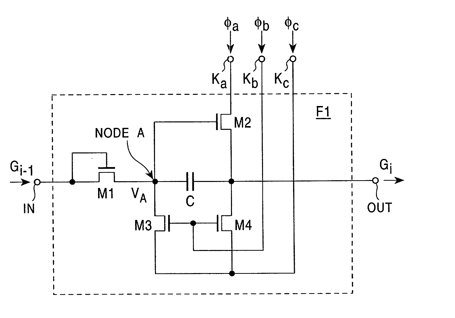
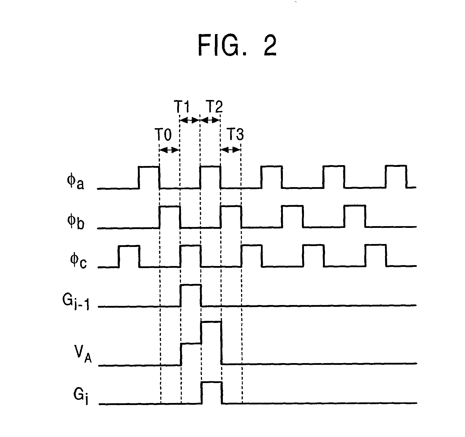
[0040] FIG. 1 is a circuit diagram which illustrates the internal circuitry of a stage F1 incorporated in a shift register according to the present invention. The stage F1 includes an input terminal IN at which a signal G.sub.i-1 output from a previous stage is input, an output terminal OUT at which a signal G.sub.i is output to a subsequent stage, and three clock input terminals K.sub.a, K.sub.b, and K.sub.c at which three-phase clock signals .phi..sub.a, .phi..sub.b, and .phi..sub.c are input, respectively.

[0041] The input terminal IN is connected to a first end (node A) of a capacitor C serving as a storage element via an MIS (metal-insulator-semiconductor) transistor M1 serving as a diode. A second end of the capacitor C is connected to the output terminal OUT. The clock input terminal K.sub.a is connected to the drain of an MIS transistor M2, the clock input terminal K.sub.b is connected to the gates of MIS transistors M3 and M4, and the clock input terminal K.sub.c is connecte...

third embodiment

[0059] FIG. 8 is an overall view of the shift register according to the The shift register is formed of a plurality of stages F'1, F'2, F'3, and the like, and the two-phase clock signals .phi..sub.a and .phi..sub.b are alternately input to the stages F'1, F'2, F'3, and the like in turn. For example, the clock signal .phi..sub.a is input to the stage F'1, and the clock signal .phi..sub.b is input to the stage F'2. A signal output from the next stage is input to the terminal K.sub.g of each of the stages F'1, F'2, F'3, and the like. For example, a signal G.sub.2 output from the next stage F'2 is input to the terminal K.sub.g of the stage F'1. This structure only requires the two-phase clock signals .phi..sub.a and .phi..sub.b to drive the shift register, thereby further reducing the number of lines in the shift register, while simplifying the clock generation circuit.

fourth embodiment

[0060] FIG. 9 is an overall view of a shift register according to the present invention. Three out of four-phase clock signals .phi..sub.a, .phi..sub.b, .phi..sub.c, and .phi..sub.d are supplied to each stage in the shift register. For example, the clock signals .phi..sub.b, .phi..sub.c, and .phi..sub.d are supplied to a stage F"1.

[0061] FIG. 10 is a timing chart of the stage F"1 shown in FIG. 9. The stage F"1 receives three of the four-phase clock signals .phi..sub.a, .phi..sub.b, .phi..sub.c, and .phi..sub.d, i.e., the clock signals .phi..sub.b, .phi..sub.c, and .phi..sub.d, and works similarly to the stage F1 according to the first embodiment.

[0062] FIG. 11 is a comparative table which illustrates the effect of reducing a delay with respect to the clock signals in the display. It is assumed that the display is a 6-inch VGA panel, and a gate driver (shift register) for driving scan lines has 480 stages with the overall length of approximately 91 mm. It is further assumed that the ...


PUM

PropertyMeasurementUnit
lengthaaaaaaaaaa
sheet resistanceaaaaaaaaaa
widthaaaaaaaaaa

Abstract

A shift register has m stages which store one of two states, where m is an integer more than 1, each stage including clock input terminals at which n-phase clock signals are input, where n is an integer more than 1, and an input terminal, and an output terminal. The input terminal of one stage receives the signal delivered from an input terminal of the shift register or from the output terminal of the previous stage. The signal output at the output terminal of one stage is passed to the input terminal of the subsequent stage or to an output terminal of the shift register. Each stage receives an initial state level from one of the clock input terminals. The initial state level is used to initialize the state of each stage.

Description

BACKGROUND OF THE INVENTION[0001] 1. Field of the Invention[0002] The present invention relates to a shift register and a device, such as a display or an image sensor, using the same.[0003] 2. Description of the Related Art[0004] FIG. 14 is a circuit diagram which illustrates the internal circuitry of a stage F101 incorporated in a conventional exemplary shift register. The stage F101 includes an input terminal IN at which a signal G.sub.i-1 output from a previous stage is input, an output terminal OUT at which a signal G.sub.i is output to a subsequent stage, clock input terminals K.sub.a and K.sub.b at which clock signals .phi..sub.a and .phi..sub.b are input, respectively, and a ground terminal GND connected to a ground potential.[0005] FIG. 15 is an overall view of the conventional exemplary shift register. The shift register is formed of a plurality of stages F101, F102, F103, and the like. The internal circuitry of the stages F102, F103, and the like is the same as that of the...

Claims


Application Information

Patent Timeline
Patent Type & Authority Applications(United States)
IPC IPC(8): G09G3/20G02F1/133G09G3/36G11C19/00G11C19/18G11C19/28H01L27/146H04N5/335H04N5/369H04N5/66
CPCG11C19/18G09G3/36
Inventor KAWAHATA, KEN
Owner MIND FUSION LLC
Why Eureka
Try Eureka