Nematic liquid crystal devices, and methods of production thereof

a liquid crystal device and nematic technology, applied in the direction of liquid crystal compositions, instruments, chemistry apparatus and processes, etc., can solve the problems of reducing yield, reducing yield, and just observing the alignment layer can produce occasional failures, and achieve the effect of reducing yield and low voltage nucleation

Inactive Publication Date: 2002-09-12
SHARP KK
View PDF6 Cites 7 Cited by
  • Summary
  • Abstract
  • Description
  • Claims
  • Application Information

AI Technical Summary

Benefits of technology

0024] Techniques for the nucleation of the operating V-state from the ground H-state are given in prior art documents EP 0,996,028; EP 0,965,876; JP-A-990432; and JP-A-9218411 mentioned above. EP 0,996,028 and EP 0,965,876 particularly teach modifying surface pretilt to obtain low voltage nucleation. However patterning just at an alignment layer can produce occasional failure (and hence reduced yield) due to disclination trapping at the surface. Methods described in JP-A-990432 and JP-A-9218411 do not have these problems, but for each to work effectively the device is ideally cooled from the isotropic phase under an applied field (to provide the correct anisotropic structure around the spacer ball or pillar); this proves to be a difficult industrial process. The alternative that is disclosed in EP 0,996,028 of in situ polymerisation under an applied field has the same industrial difficulty. This invention offers a solution by providing a preformed anisotropic protrusion.

Problems solved by technology

However patterning just at an alignment layer can produce occasional failure (and hence reduced yield) due to disclination trapping at the surface.
Methods described in JP-A-990432 and JP-A-9218411 do not have these problems, but for each to work effectively the device is ideally cooled from the isotropic phase under an applied field (to provide the correct anisotropic structure around the spacer ball or pillar); this proves to be a difficult industrial process.

Method used


Image

  • Nematic liquid crystal devices, and methods of production thereof
  • Nematic liquid crystal devices, and methods of production thereof
  • Nematic liquid crystal devices, and methods of production thereof

Examples


first embodiment

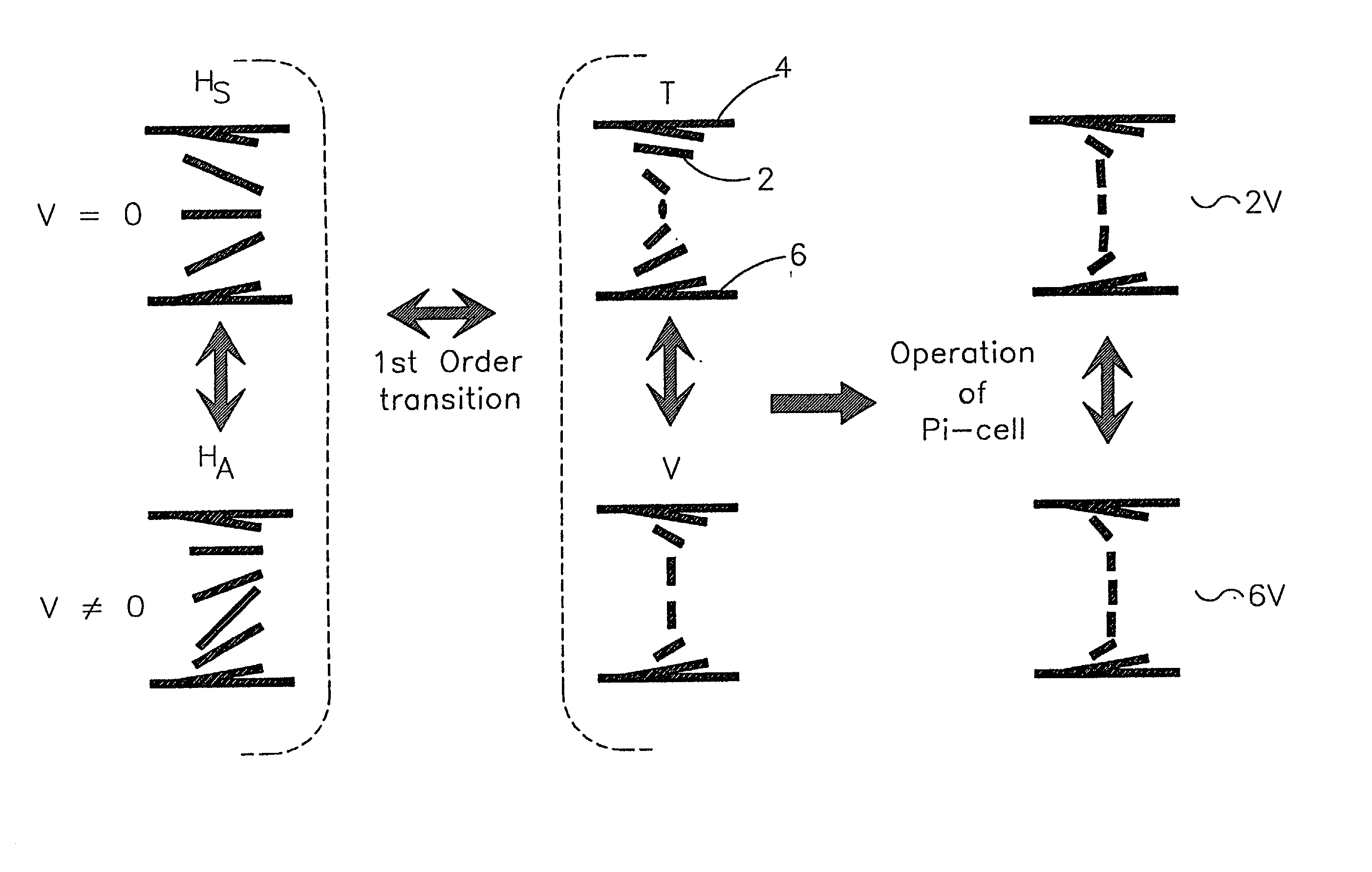
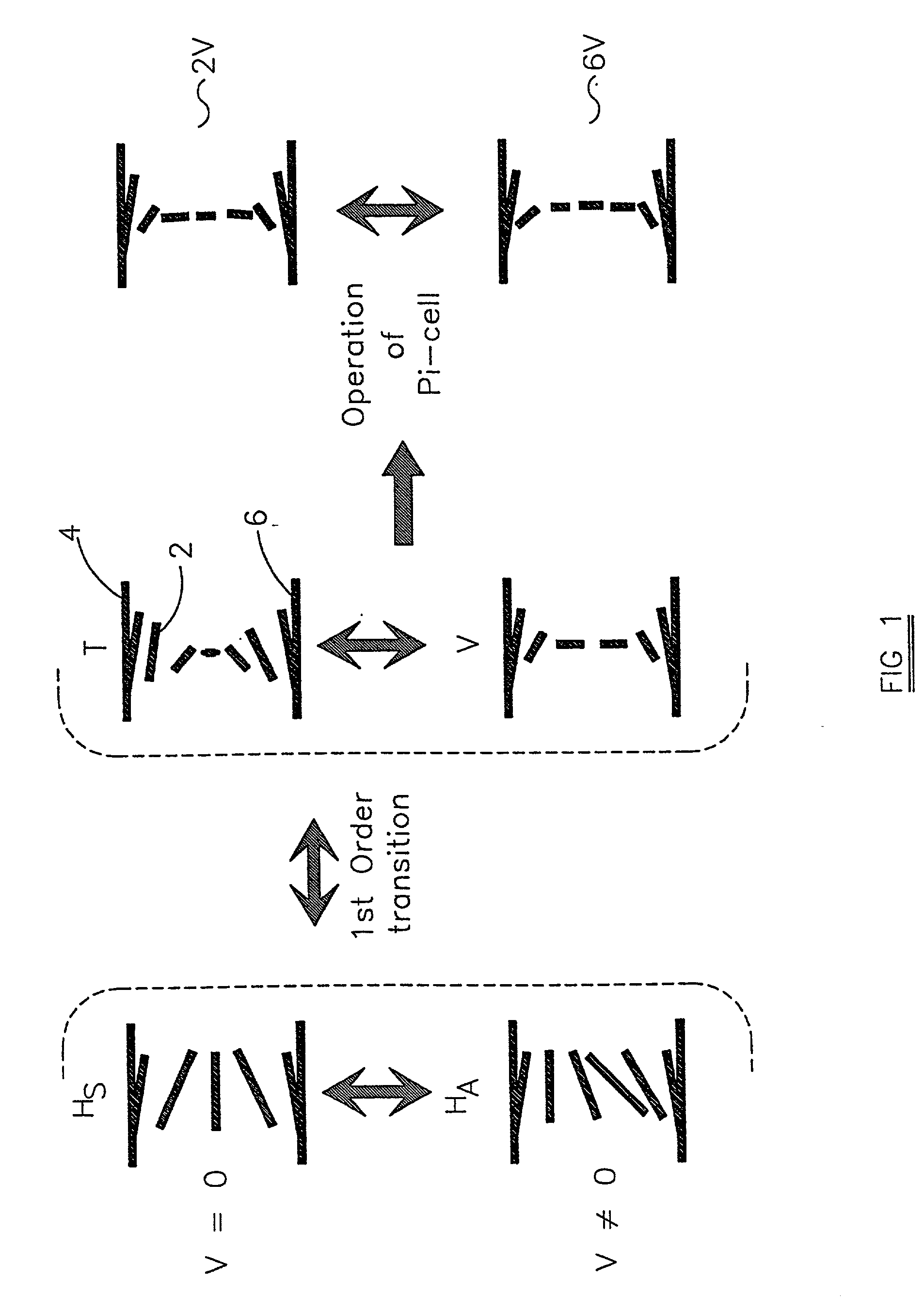
[0034] the invention uses twisted anisotropic protrusions to nucleate V-state from H-state.

[0035] Referring to FIG. 3a, two indium tin oxide glass coated substrates 30 and 42 were coated, as known to those skilled in the art, with alignment layers 32 and 33 formed from SE610 (Nissan chemicals). Each substrate 30, 42 was then unidirectionally rubbed again as known to those skilled in the art. Referring to FIG. 3b, on one of these substrates 30 a mixture of 1:3 reactive mesogen RM257 (Merck) to toluene was spun at 1200 rpm (at 80.degree. C.), the RM257 being previously doped with 1.2% CB15 (Merck) to form a protrusion layer 34. Again at 80.degree. C. the RM257 / CB15 protrusion layer 34 was UV cured through a mask 36 by UV radiation 38, and then rinsed in toluene to leave one substrate 30 coated with about 2.5 micron high twisted anisotropic protrusions 40, as shown in FIG. 3c. This substrate 30 was then fabricated into a 5 micron thick pi-cell using the other substrate 42, as shown in ...

second embodiment

[0038] the invention uses tilted anisotropic protrusions to nucleate V-state from H-state Referring again to FIGS. 3a to 3d, and using the same reference numerals for simplicity, two indium tin oxide glass coated substrates 30 and 42 were coated, as known to those skilled in the art, with alignment layers 32 and 33 formed from SE610 (Nissan chemicals). Each substrate 30, 42 was then unidirectionally rubbed again as known to those skilled in the art (FIG. 3a). On one of these substrates 30 a mixture of 4:1:15 diacrylate RM257 (Merck) to monoacrylate RM308 (Merck) to toluene was spun at 1200 rpm (at 80.degree. C.) to form a protrusion layer 34. Again at 80.degree. C. the RM257 / RM308 protrusion layer 34 was UV cured through a mask (FIG. 3b) and then rinsed in toluene to leave one substrate 30 coated with about 2.5 micron high tilted anisotropic protrusions 40 (FIG. 3c). This substrate 30 was then fabricated into a 5-micron thick pi-cell using the other substrate 42 as shown in FIG. 3d....

fourth embodiment

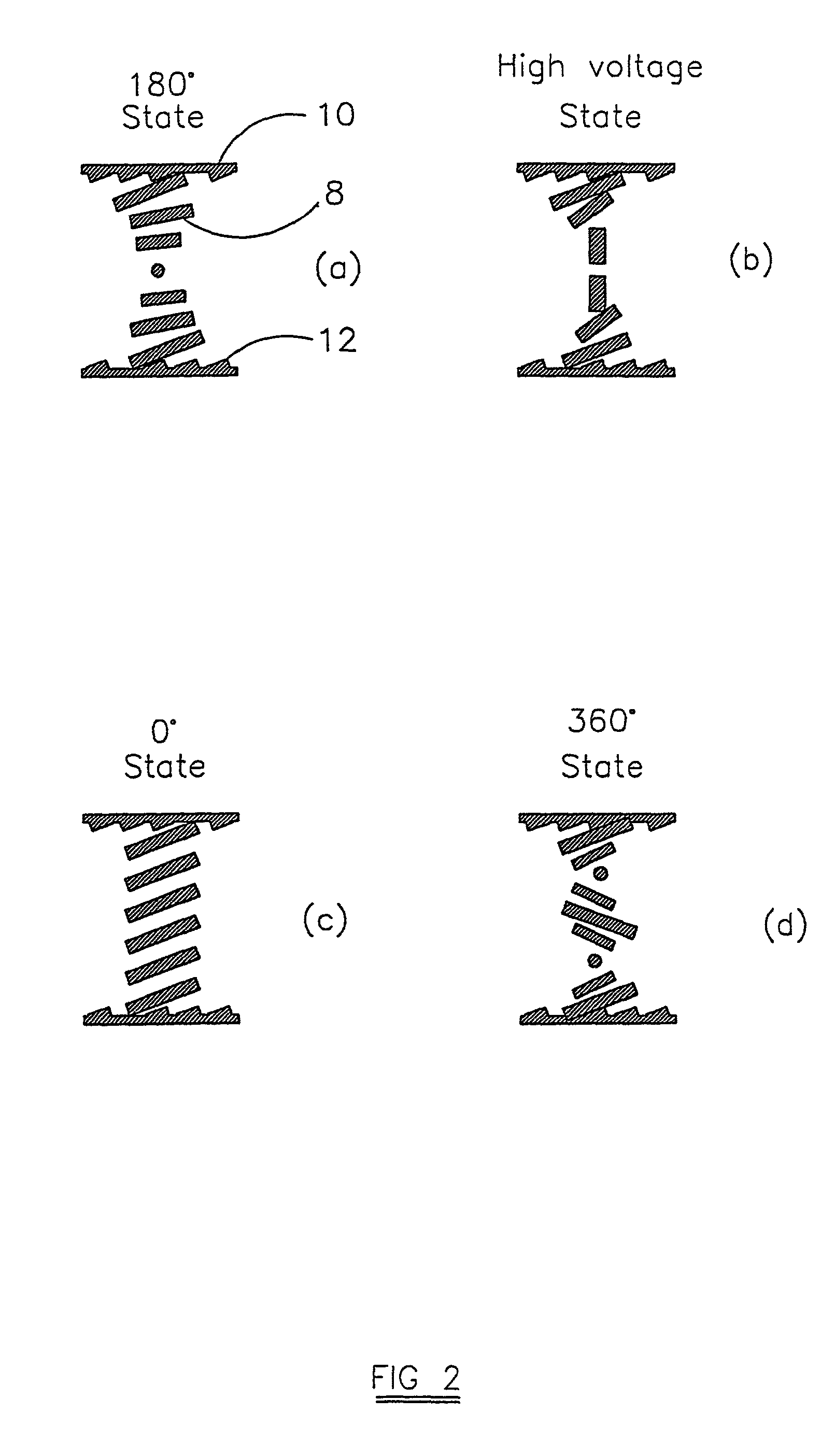
[0043] the invention uses tilted anisotropic protrusions for isolation of states in a BTN Device. We have found that tilted anisotropic protrusions also act as isolation regions in BTN devices. In this case each pixel of a display panel is fully surrounded by such a protrusion.


PUM

PropertyMeasurementUnit
thickaaaaaaaaaa
voltageaaaaaaaaaa
anisotropicaaaaaaaaaa

Abstract

A liquid crystal device comprises a nematic liquid crystal, voltage means for applying a voltage across said liquid crystal, and two substrates (42, 30) each provided with an alignment layer (32, 33), wherein: said liquid crystal is sandwiched between said two substrates (42, 30); said nematic liquid crystal can be placed in at least one operating state and at least one non-operating state, and at least one of said alignment layers (32, 33) is provided with a plurality of surface protrusions (40) formed from an anisotropic material.

Description

BACKGROUND OF THE INVENTION[0001] 1. Field of the Invention[0002] The invention relates to nematic liquid crystal devices formed with anisotropic protrusions, and methods of production. thereof.[0003] 2. Description of the Related Art[0004] The invention can be used to provide an improvement in obtaining and if necessary isolating the operating state of a pi-cell liquid crystal device at low voltages. The invention can also be applied to nucleating the operating states from the globally stable states in the BTN device, and for isolating the operating states from each other and from the globally stable state.[0005] The invention is particularly applicable to flat panel displays and pi-cells used in LCTV. Another application is in using BTN displays in mobile products.[0006] P. D. Berezin, L. M. Blinov, I. N. Kompanets and V. V. Nikitin `Electro-optic Switching in Oriented Liquid-Crystal Films` July-August 1973 Sov. J. Quant. Electron Vol. 3, pp. 78-79 is a paper which describes the a...

Claims


Application Information

Patent Timeline
Patent Type & Authority Applications(United States)
IPC IPC(8): G02F1/13G02F1/1333G02F1/1337G02F1/139
CPCG02F1/1337G02F1/133707G02F1/133753G02F1/1391G02F1/1395G02F2001/133726G02F2001/133776G02F1/133726G02F1/133776G02F1/13
Inventor TOWLER, MICHAEL JOHNACOSTA, ELIZABETH JANE
Owner SHARP KK
Why Eureka
Try Eureka