Submicron thermal imaging method and enhanced resolution (super-resolved) ac-coupled imaging for thermal inspection of integrated circuits

a thermal inspection and integrated circuit technology, applied in the field of noncontact thermal registration methods, can solve the problems of inability to accurately and accurately measure the temperature of the integrated circuit, the required sophistication of the experimental setup, and the lack of accuracy, etc., to achieve simple and inexpensive temperature measurements and high spatial resolution

Active Publication Date: 2002-09-12
RGT UNIV OF CALIFORNIA
View PDF5 Cites 94 Cited by
  • Summary
  • Abstract
  • Description
  • Claims
  • Application Information

AI Technical Summary

Benefits of technology

[0019] The present invention includes an AC-coupled thermoreflectance method for performing simple and inexpensive temperature measurements of samples having a known surface material composition that can provide spatial resolution at better than one micron, and thermal resolution to about 10 mK.degree. or better. The method is particularly well-suited for use on small geometry active devices (micron and sub micron regimes), such as integrated circuits, MEMs devices, HIT devices, and other small scale active devices whose thermal activity may be modulated, and for which thermal profiles need to be accurately profiled, or imaged. To obtain high spatial resolution the present the thermoreflectance method of the present invention preferably utilizes two dimensional optical detector arrays, such as CMOS detector arrays, or PIN-array detectors, which are coupled with parallel processing of the image data. It will be appreciated that a detector array is not subject to the non-repeatability of mechanical positioning which is characteristic of point, and point scanning thermal measurements.
[0022] The use of the AC coupling in the method of the invention increases the effective signal-to-noise ratio. Registration of the small thermoreflectance signal is preferably accomplished within the present invention by utilizing differential box-car filtering, lock-in amplification, FFT analysis, and other differencing and / or very narrow band signal filtering techniques. A thermoreflectance microscope built according to the invention can provide thermal images of micron and sub micron regions and high thermal sensitivities extending to about 10 mK.degree. and the technique may be utilized down to cryogenic temperatures.
[0023] This resultant thermoreflectance microscope according to the present invention can generate quantitative, real time thermal images with a higher spatial resolution than any commercially available infrared microscope. To obtain quantitative measurements, signal processing must be performed on the data, but this is not much more complicated than what is currently required for infrared imaging and still allows for a "real-time" image. Also, the resultant thermoreflectance microscope can be utilized at very low temperatures where insufficient blackbody signal exists for use by infrared cameras. For example, thermoreflectance imaging may be the only viable non-contact method to measure the temperature on an active semiconductor in a cryostat. It will be appreciated that a number of advantages are provided by the use of a thermoreflectance microscope according to the present invention.
[0024] Another aspect of the invention is a method and apparatus for further enhancing the resolution of thermoreflective imaging. This method uses multiple images of the device together with a technique for combining the images using an interpolation routine executing on a processor, or other processing element capable of manipulating image data, to obtain spatial resolution beyond that given directly by the imaging system hardware. In effect, the invention produces high resolution images from a lower resolution camera by intelligently collecting and combining multiple images gathered by carefully controlled relative motion between the device and the camera. The method will allow measurement of image details with unprecedented resolution up to approximately 0.2 .mu.m, and perhaps reaching increased spatial resolution at or below 0.1 .mu.m under favorable conditions. Although techniques have existed for enhancing resolution from multiple frames, the use of superresolution imaging for these AC-coupled imagers in combination with implementation of the present techniques, and the scanning and imaging apparatus, is inventive and provides significant benefits. The technique can be applied to applications such as thermal imaging of small circuits and devices which can achieve sub-micron spatial resolution and 10 mK.degree. to 50 mK.degree. temperature resolution.

Problems solved by technology

Although a number of methods exist to measure the temperature on such a small scale, all current methods suffer from one or more shortcomings, such as lack of accuracy, measurement speed, the required sophistication of the experimental setup, and complexity of the required data analysis.
Use of a thermocouple has a number of drawbacks which are primary result of its significant size in relation to the device under test, which in this case is a HIT cooler, such as in the 10 .mu.m to 100 .mu.m size range.
Furthermore, the thermocouples require the careful use of thermal pastes and are susceptible to breakage.
Moderate complexity image processing is required to recover the relative temperature map.
In addition, accuracy depends on considerations of layer thickness and possible non-uniformities.
The spatial resolution is limited by the size of the laser spot of the interfometer.
The probe is then placed close enough to the surface of the device and the near field can be transmitted through the fiber-optic, subject to a level of intrinsic loss.
A few of the complications involved with the method are issues relating to the construction of the fiber optic probe, and its placement in sufficient proximity to the surface of the device to measure the near field.
Typically, this requirement can be met by positioning the probe within 25 nm of the surface; however, any sudden contact with the surface can easily destroy the probe.
The generation of accurate thermal images, therefore, requires a knowledge of the emissivity for each element within the image, which consequently complicates temperature calibration of the associated infrared camera images.
It was found, however, that even from a camera costing over one hundred thousand dollars, the image was not useful even on the largest coolers.
However, in all these instances the small thermoreflectance coefficient results in the generation of a measurement having a low signal-to-noise ratio, and the technique is unable to provide absolute measurements.
Therefore, it will be appreciated current methods for performing thermal measurements on small circuits and devices are difficult to construct and calibrate, while they often provide insufficient spatial and thermal resolution.

Method used


Image

  • Submicron thermal imaging method and enhanced resolution (super-resolved) ac-coupled imaging for thermal inspection of integrated circuits
  • Submicron thermal imaging method and enhanced resolution (super-resolved) ac-coupled imaging for thermal inspection of integrated circuits
  • Submicron thermal imaging method and enhanced resolution (super-resolved) ac-coupled imaging for thermal inspection of integrated circuits

Examples


Embodiment Construction

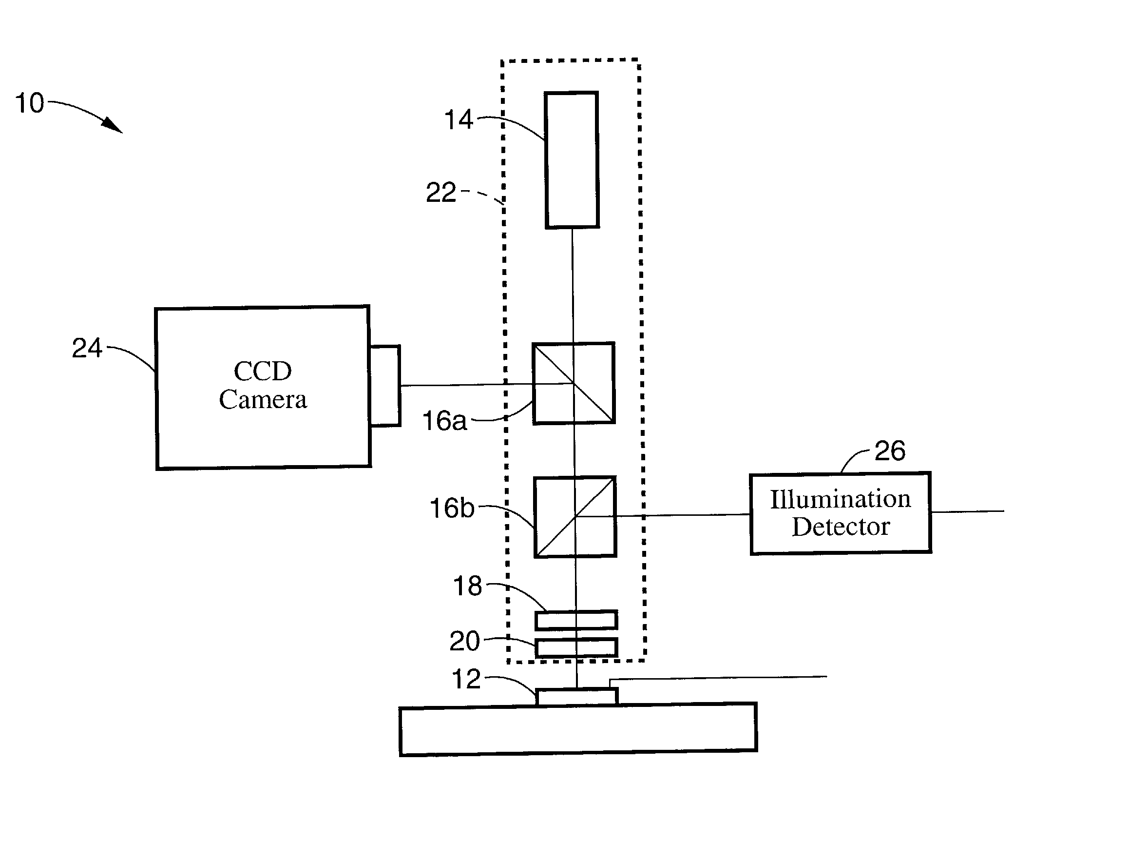
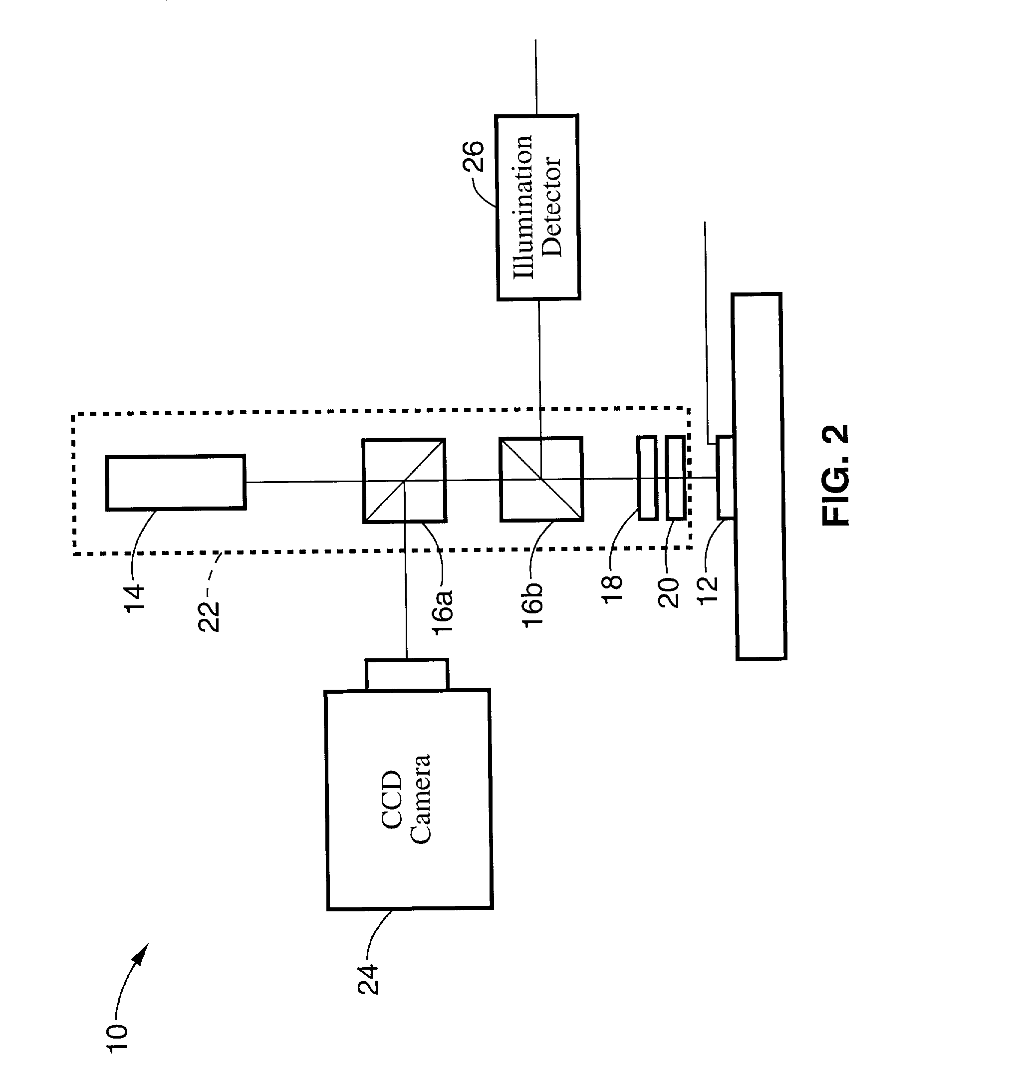
[0053] For illustrative purposes the present invention is embodied in the apparatus and methods described herein with reference to FIG. 1 through FIG. 15. It will be appreciated that the apparatus may vary as to configuration and as to details of the parts, and that the method may vary as to the specific steps and sequence, without departing from the basic concepts as disclosed herein.

[0054] 1. Introduction.

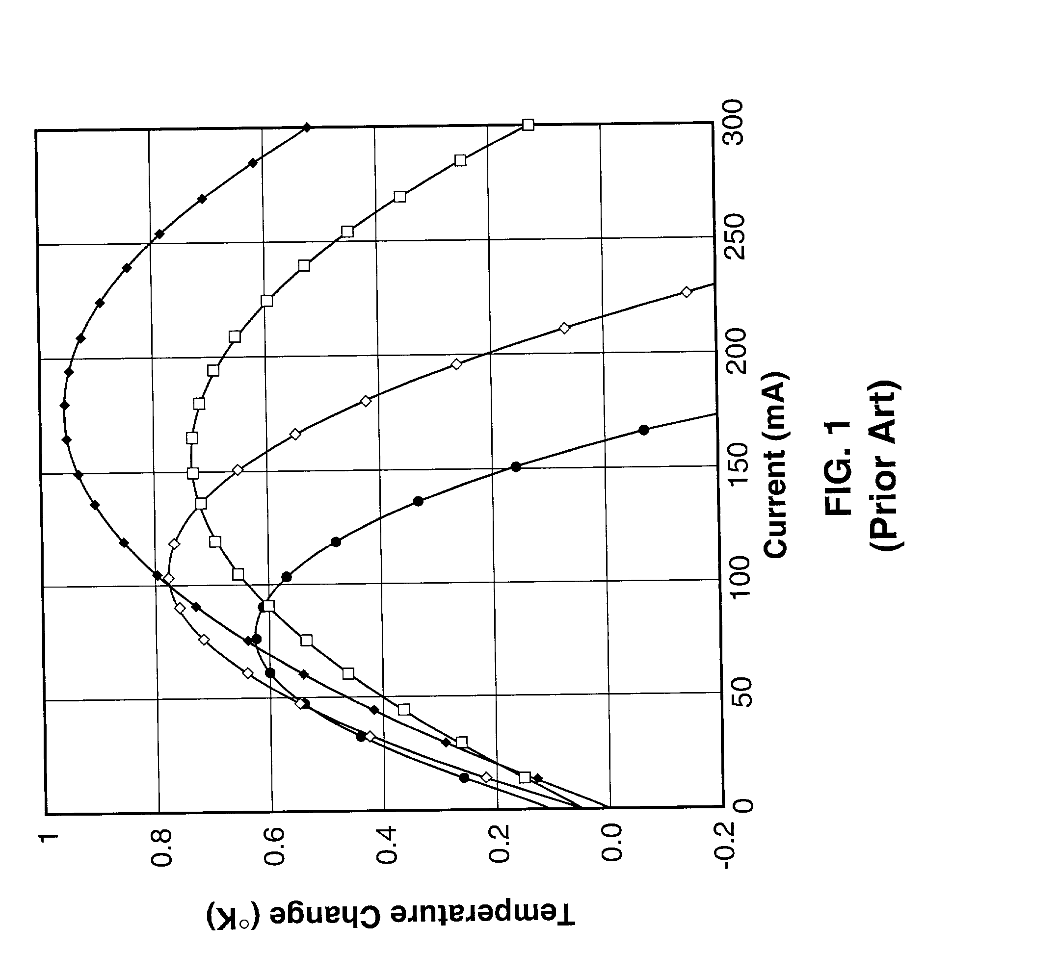
[0055] The thermoreflectance method of the present invention relies on the fact that the reflection of a surface is dependent on its temperature. Thermoreflectance refers to excitation from an external source, wherein a relative change of reflectance is measured. Previous use of thermoreflectance as a measure of thermal excitation required that the surface be subject to a high temperature change, such as within the metal traces. Typically the previous thermoreflectance methods were capable of providing measurements of temperature change on the order of 10 degrees or more, and wer...


PUM


Abstract

Methods and apparatus for non-contact thermal measurement which are capable of providing sub micron surface thermal characterization of samples, such as active semiconductor devices. The method obtains thermal image information by reflecting a light from a surface of a device in synchronous with the modulation of the thermal excitation and then acquiring and processing an AC-coupled thermoreflective image. The method may be utilized for making measurements using different positioning techniques, such as point measurements, surface scanning, two-dimensional imaging, and combinations thereof. A superresolution method is also described for increasing the resultant image resolution, based on multiple images with fractional pixel offsets, without the need to increase the resolution of the image detectors being utilized. The thermoreflective method provides a spatial resolution better than current infrared cameras, operates within a wide temperature range, and is capable of a thermal resolution on the order of 10 mK.degree..

Description

BACKGROUND OF THE INVENTION[0001] 1. Field of the Invention[0002] This invention pertains generally to non-contact thermal registration methods, and more particularly to high resolution and super-resolution non-contact optical methods for providing thermal sub micron characterization of active semiconductor devices.[0003] 2. Description of the Background Art[0004] Advances are continually being made in semiconductor fabrication techniques that allow manufacturing smaller and faster semiconductor devices. It will be appreciated that these fast-switching devices also can generate an increasing amount of heat per unit area. Effective thermal management, therefore, is essential to achieve reliable operation of these semiconductor devices in the face of continuing advancement, and the characterization of thermal effects on the scale of these devices is becoming increasing important. It will be appreciated that achieving temperature measurements on increasingly smaller device geometries i...

Claims


Application Information

Patent Timeline
Patent Type & Authority Applications(United States)
IPC IPC(8): G01J5/00
CPCG01J5/00G01J5/0096G01J5/08G01J5/0862G01J5/0896G01J5/58G01J2005/0077G01J5/0802
Inventor SHAKOURI, ALIMILANFAR, PEYMANPEDROTTI, KENNETHCHRISTOFFERSON, JAMES
Owner RGT UNIV OF CALIFORNIA
Why Eureka
Try Eureka