Method and apparatus for measurements of patterned structures

a patterned structure and measurement method technology, applied in the field of measurement techniques, can solve problems such as difficult to solve, optical system bullying and complicated, and exclude it from continued processing

Inactive Publication Date: 2002-09-12
NOVA MEASURING INSTR LTD
View PDF19 Cites 15 Cited by
  • Summary
  • Abstract
  • Description
  • Claims
  • Application Information

AI Technical Summary

Benefits of technology

0025] effects due to limited coherence of illumination;
0026] interference between light beams reflected from each stack within the grid cycle, taking into account the above effects.
0027] The contribution of each of the above effects into the theoretical data axe estimated in accordance with the known physical laws.
0028] The optical model, being based on some of the features, actually requires certain optical model actors to be considered in order to perform precise calculations of the desired parameters. If information of all the features is not available and the model cannot be optimized prior to the measurements, this is done by means of a lo so-called initial "learning" step. More specifically, there are some optical model factors which, on the one hand, depend variably on all the features and, on the other hand, define the contribution of each of the existing optical effects into the detected signal. The values of these optical model factors are adjusted along with the unknown desired parameters during the learning step so as to satisfy the predetermined condition The latter is typically in the form of a merit function defining a so-called "goodness of fit" between the measured and theoretical data. The resulting optical model factors can consequently be used in conjunction with known features to enable precise calculations of the desired parameters of the structure.
0029] Preferably, the measurement area is the part of the structure to be measured. Alternatively, the measurement area is located on a test pattern representative of the actual structure to be measured, namely having the same design rules and layer stacks. The need for such a test pattern may be caused by one of the following two reasons:
0030] 1) If the measurement area is not substantially smaller than he available surface area defined by the actual structure to be measured, then the test site is implemented so as to include an extended structure;

Problems solved by technology

Certain measuring techniques enable the local dimensions of a wafer to be measured with relatively high resolution, but at he expense of discontinued use of the wafer in production.
For example, inspection using a scanning electron microscope gives measurements of the parameters of a patterned structure, brut at the expense of cleaving it and thus excluding it from continued processing.
Unfortunately, in the case of a very small structure, this approach suffers from a common drawback associated, on the one hand, with the use of a small spot-size and, on the other hand, owing to the large numerical aperture, with the collection of high diffraction orders.
This leads to various problems, which are difficult to solve.
Indeed, not all the stacks' layers are in the focus of an optical system used for collecting reflected light, the optical system being bully and complicated.
Diffraction effects, which depend significantly on the gird profile and topography and therefore are difficult to model, have to be included in calculations.
However, a large number of test areas are used and also information on multiple parameters cannot be obtained.
However, it is often the case that the structure under inspection is such that the different portions cannot be separately imaged.
This is owing to an unavoidable limitation associated with the diameter of a beam of incident radiation striking the structure.
This is not feasible for layers of small thickness and small thickness difference because of a limited number of reflection oscillations.
For many processes in the field such as etching and photoresist development; this assumption is incorrect and this method is therefor inapplicable.

Method used


Image

  • Method and apparatus for measurements of patterned structures
  • Method and apparatus for measurements of patterned structures
  • Method and apparatus for measurements of patterned structures

Examples


Embodiment Construction

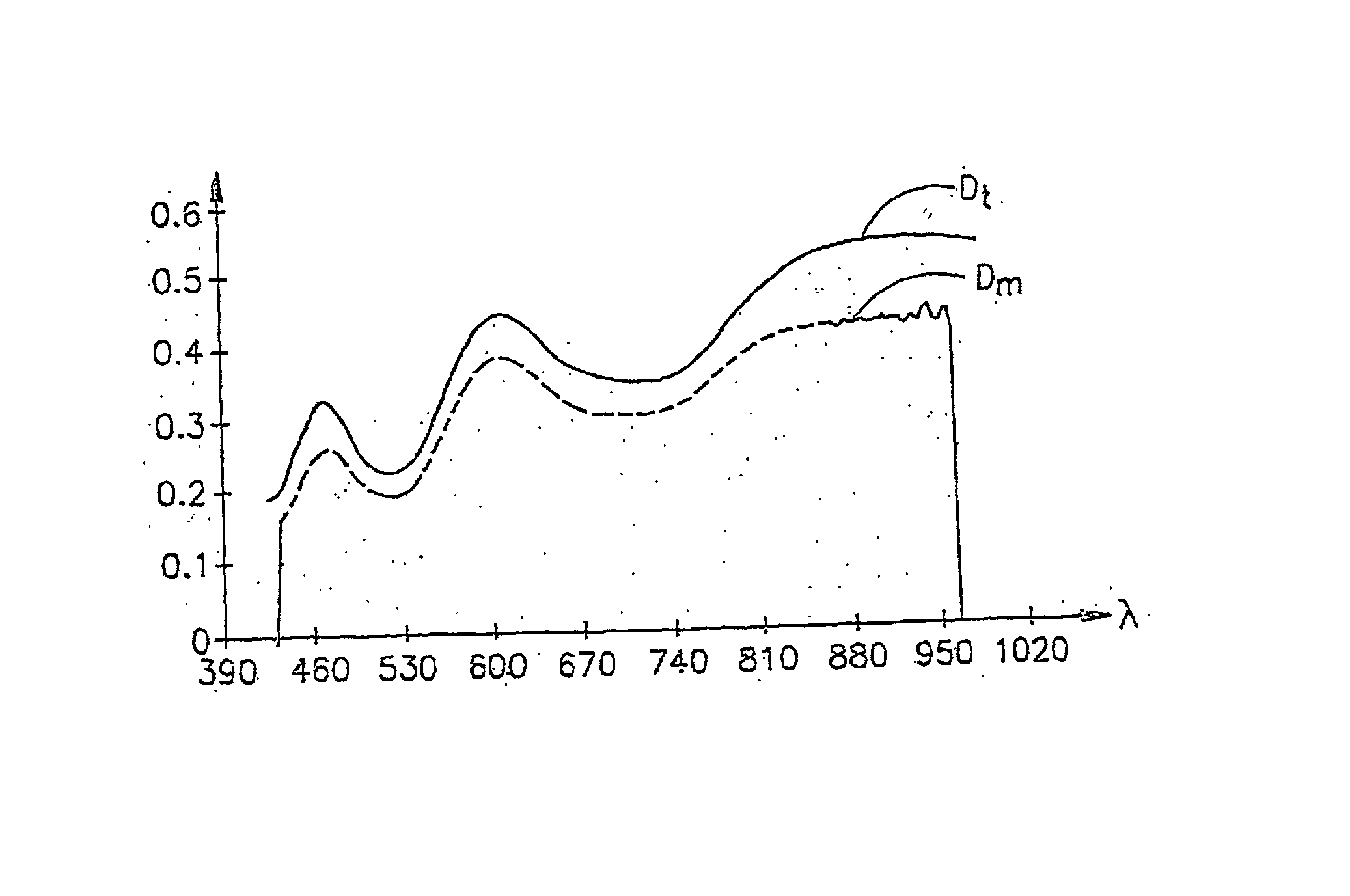
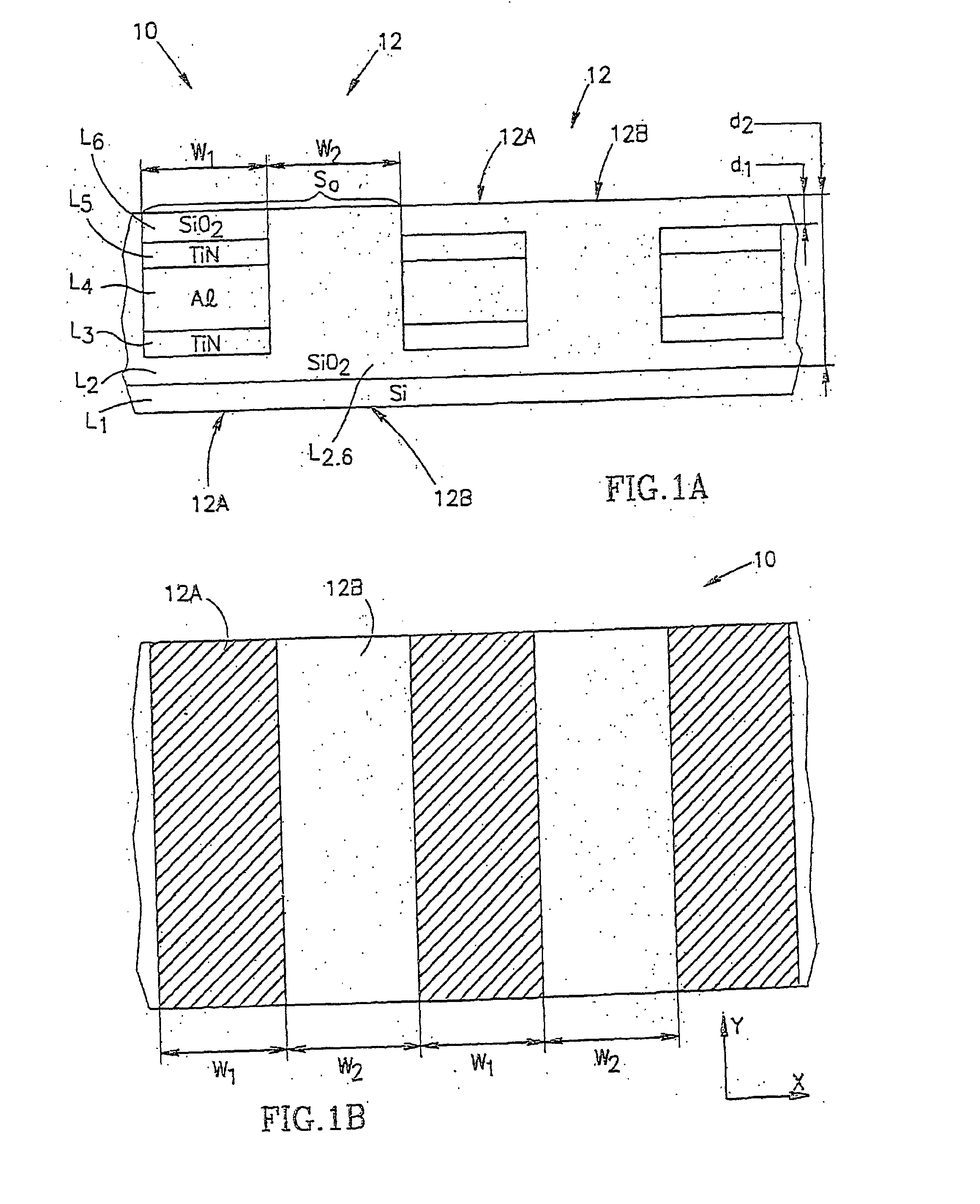
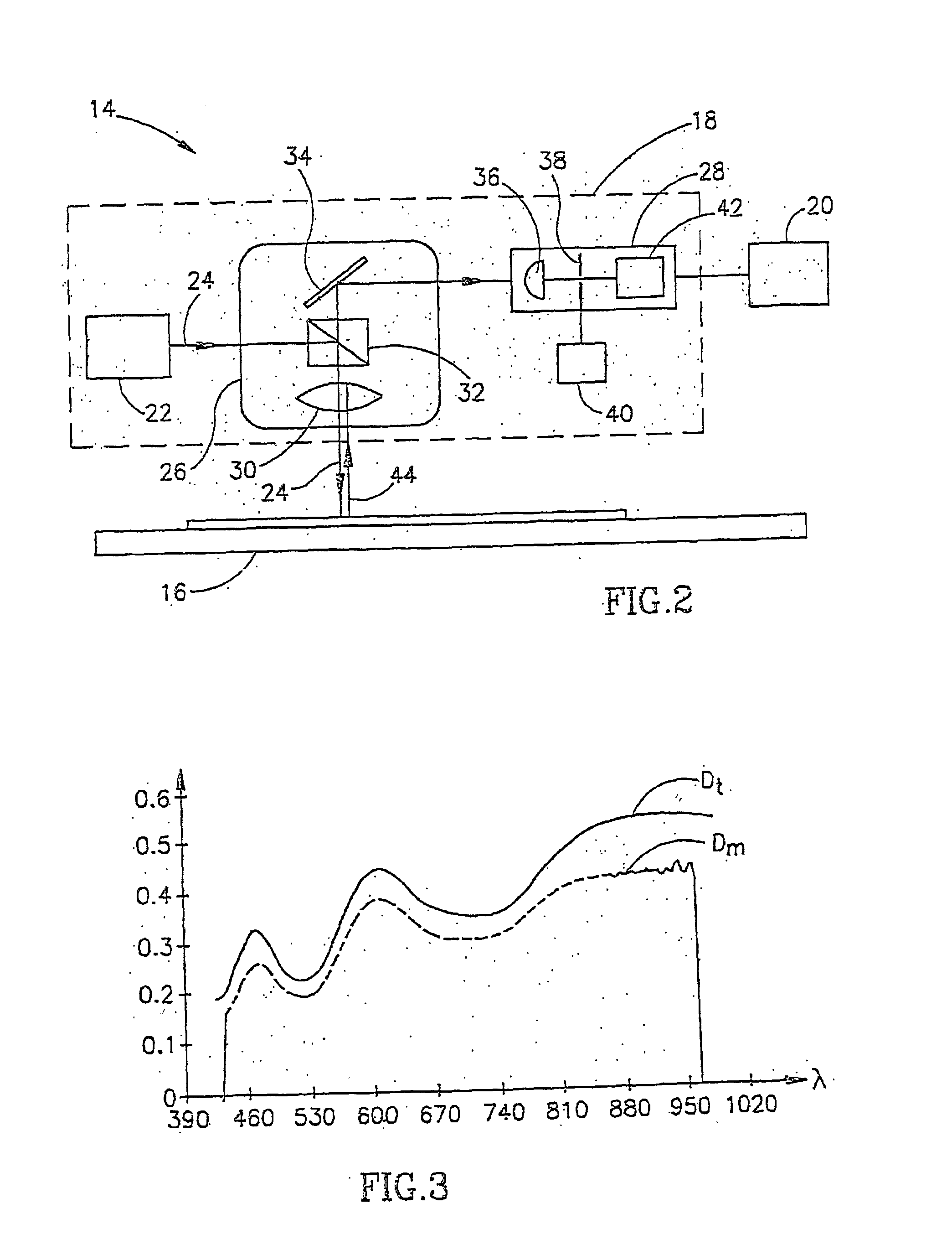
[0050] Referring to FIGS. 1a and 1b, there are partly illustrated a cross-section and a top view, respectively, of a grid-like wafer structure, generally designated 10, whose parameters are to be measured. The structure is formed of a plurality of cells, generally at 12, each constituting a grid cycle. Only three adjacent cells 12 are demonstrated in the present example with only two stacks (or elements) in each cell in order to simplify the illustration. Thus, the cell 12 comprises two stacks 12a and 12b formed of different layers. More specifically, the stack 12a includes six layers L.sub.1-L.sub.6, wherein the layers L.sub.1 and L.sub.2 and the layer L.sub.6 form two layers L.sub.1 and L.sub.2,6, respectively, of the stack 12b. As known in the conventional semiconductor devices, semiconductor structures such as sources, drains and gate electrodes, capacitors, etc. are formed in and on a semiconductor substrate (layer L.sub.1) typically made of silicon material and including metal...


PUM


Abstract

A method for measuring at least one desired parameter of a patterned structure having a plurality of features defined by a certain process of its manufacturing. The structure represents a grid having at least one cycle formed of at least two metal-containing regions spaced by substantially transparent regions with respect to incident light defining a waveguide. An optical model is provided, which is based on at least some of the features of the structure defined by a certain process of its manufacturing, and on the relation between a range of the wavelengths of incident radiation to be used for measurements and a space size between the two metal-containing regions in the grid cycle, and a skin depth of said metal. The model is capable of determining theoretical data representative of photometric intensities of light components of different wavelengths specularly reflected from the structure and of calculating said at least one desired parameter of the structure. A measurement is area is located and spectrophotometric measurements are applied to the measurement area, by illuminating it with incident light of a preset substantially wide wavelength range. A light component substantially specularly reflected from the measurement area is detected, and measured data representative of photometric intensifies of each wavelength within the wavelength range is obtained. The measured and theoretical data are analyzed and the optical model is optimized until the ,theoretical data satisfies a predetermined condition. Upon detecting that the predetermined condition is satisfied, said at least one parameter of the structure is calculated.

Description

FIELD OF THE INVENTION[0001] This invention is in the field of measurement techniques and relates to a method and a system for measuring the parameters of patterned structures.BACKGROUND OF THE INVENTION[0002] Techniques for thickness measurements of patterned structures have been developed. The term "patterned structure" used herein signifies a structure formed with regions having different optical properties with respect to an incident radiation. More particularly, a patterned structure represents a grid having one or more cycles, each cycle being formed of at least two different locally adjacent stacks. Each stack is comprised of layers having different optical properties.[0003] Production of integrated circuits on semiconductor wafers requires maintaining tight control over the dimensions of small structures. Certain measuring techniques enable the local dimensions of a wafer to be measured with relatively high resolution, but at he expense of discontinued use of the wafer in pr...

Claims


Application Information

Patent Timeline
Patent Type & Authority Applications(United States)
IPC IPC(8): G01B11/02G01B11/06G01J3/42H01L21/66
CPCG01B11/02G01B11/0625G01J3/42H01L22/12
Inventor SCHEINER, DAVIDMACHAVARIANI, VLADIMIR
Owner NOVA MEASURING INSTR LTD
Why Eureka
Try Eureka