

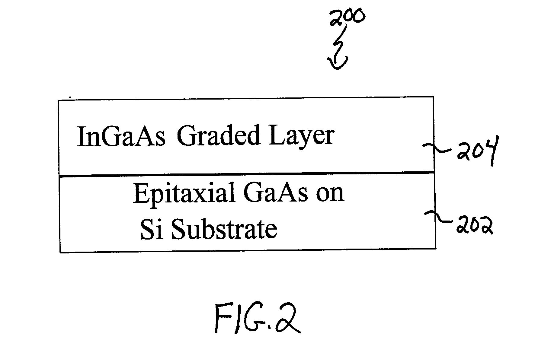
Relaxed InxGa1-xAs layers integrated with Si
a technology of xas and inxga1, which is applied in the direction of polycrystalline material growth, crystal growth process, after-treatment details, etc., can solve the problems of removing the structure of defects, and achieve the effects of low defect densities and relaxation, high temperature growth, and high quality
- Summary
- Abstract
- Description
- Claims
- Application Information
AI Technical Summary
Benefits of technology
Problems solved by technology
Method used
Image

Examples
Embodiment Construction
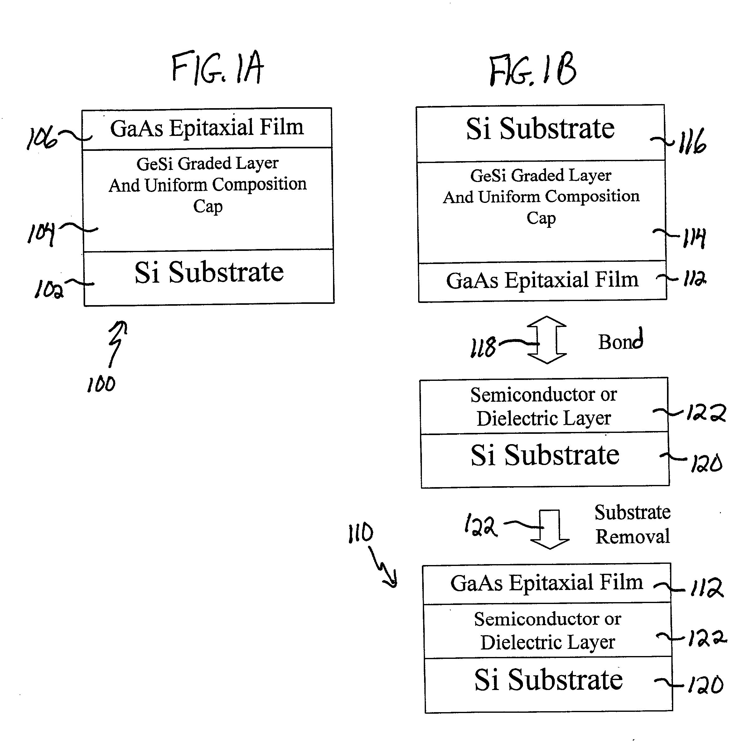
[0021] In order to produce a high quality InGaAs epitaxial film on Si, one must first produce a GaAs on Si virtual substrate. FIG. 1A shows an exemplary embodiment of a virtual substrate structure 100. The structure is produced by grading SiGe from 0 to 100% Ge and depositing a uniform cap of Ge (104) on a Si substrate 102, and thereafter depositing an epitaxial layer 106 of GaAs. Since GaAs is lattice matched to Ge, the grading procedure results in a low defect density, GaAs film. This virtual substrate growth is actually a multi-step process that involves epitaxy, planarization, and careful preparation of the Ge surface prior to the GaAs epitaxy. These processes are described in detail in Currie et. al., Appl. Phys. Lett., 72, 1718 (1998) and Ting et. al., J. Elec. Mater., 27, 451 (1998), both of which are incorporated herein by reference.
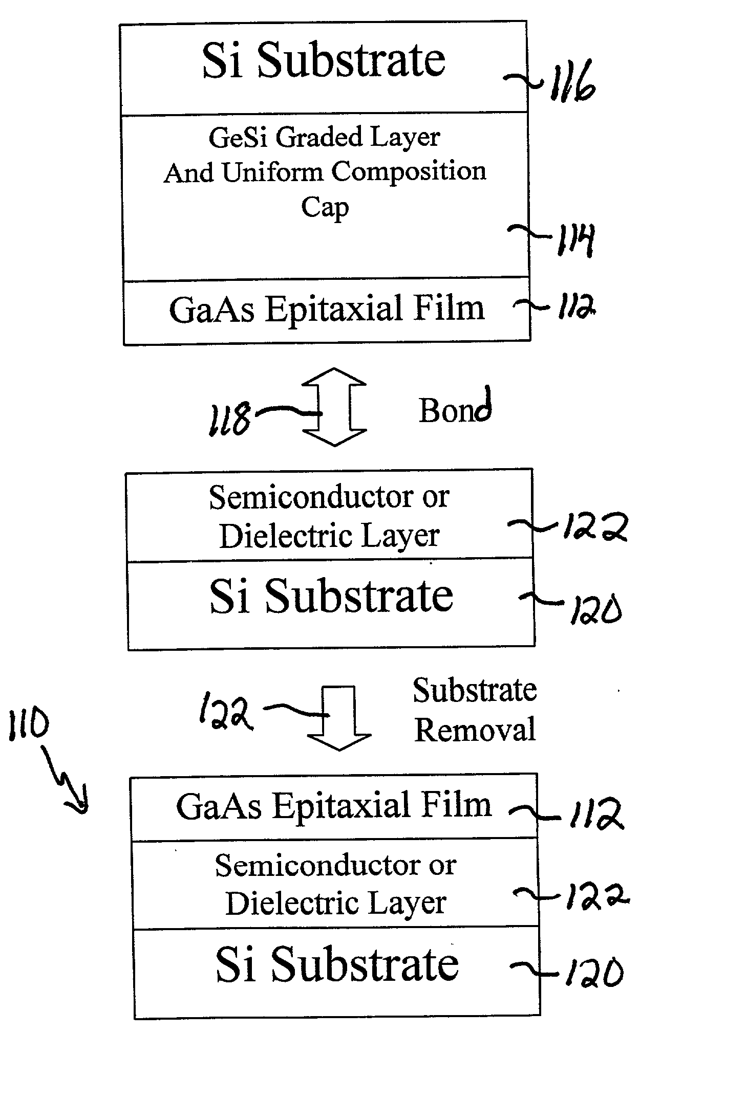
[0022] FIG. 1B is another exemplary embodiment of a GaAs virtual substrate structure 110. This structure is produced by grading SiGe to uniform ...
PUM
| Property | Measurement | Unit |
|---|---|---|
| rms roughness | aaaaa | aaaaa |
| threading dislocation density | aaaaa | aaaaa |
| composition | aaaaa | aaaaa |
Abstract
Description
Claims
Application Information