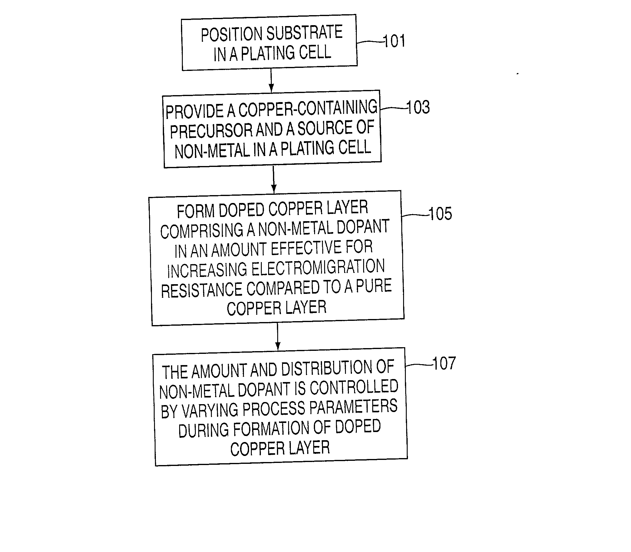
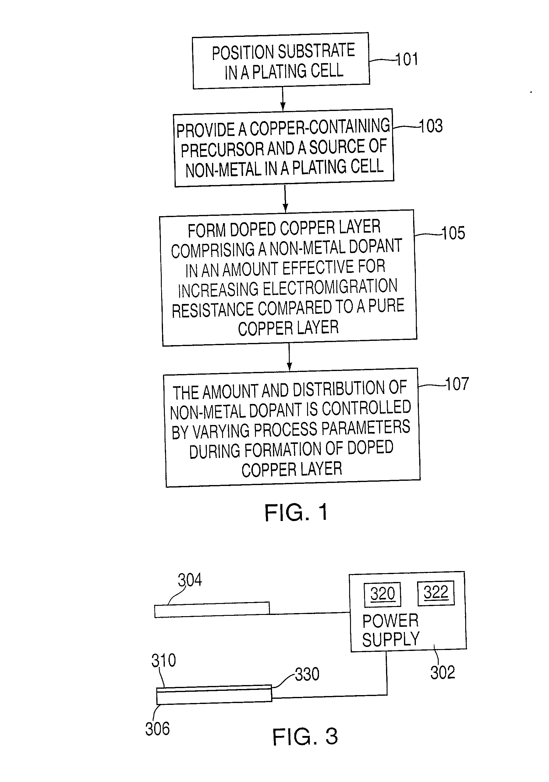
Method of forming copper interconnects
a technology of interconnects and copper, applied in the direction of electrolysis components, semiconductor/solid-state device details, coatings, etc., can solve the problems of metal line discontinuities, metal film material transport,
- Summary
- Abstract
- Description
- Claims
- Application Information
AI Technical Summary
Problems solved by technology
Method used
Image

Examples
example 1
[0039] In one embodiment, the electroplating bath comprises copper sulfate, with appropriate additives such as an accelerator, a suppressor and a chlorine-containing source for generating chloride ions. For example, copper sulfate may be present in a concentration range of between about 0.1M to about 0.9M, and the electroplating bath may have a pH ranging from about 0.6 to about 3. The activities of suppressers and accelerators depend on various parameters such as temperature, pH and chloride concentration in the electroplating bath. A stronger acid (i.e., lower pH) tends to shorten the lifetime of the additives. This electroplating bath, which has a pH that is higher than conventional baths, is referred to in this disclosure as Plating Bath A.
[0040] The additives comprise an accelerator X and a suppressor Y which are supplied by LeaRonal (now Shipley) of New York, U.S.A., as Electra plate X Rev 1.0 and Electra plate Y Rev 1.0 respectively. The accelerator X is a sulfonic acid based...
example 2
[0050] As previously mentioned, the plating pulse sequence used for carbon incorporation varies with the specific plating bath that is used. For example, a conventional electroplating bath maybe used. One example of a conventional electroplating bath is known as a Cu Bath M.TM., which is available from Enthone-OMI of New Haven, Conn. The Cu Bath M.TM. contains proprietary compounds, but typically has a pH that is about 10 times more acidic than the Plating Bath A. For example, the pH for the conventional electroplating bath maybe less than about 0.1. The inventors have found that, unlike Plating Bath A carbon incorporation using this plating bath is enhanced by using a relatively low current density for the deposition pulses. It is believed that this different dependence on the current density may be attributed to the different compounds and / or the pH used in the plating baths.
[0051] A low current DC pulse, e.g., at a current density of less than about 5 mA / cm.sup.2, preferably less...
example 3
[0054] In practicing embodiments of the invention, the deposition time durations and current density of the electrical pulses may be adjusted as appropriate to achieve desired plating results, including the total carbon content and the location of the carbon-rich layer. As such, the plating pulse sequence may also be designed to deposit several carbon-rich copper layers having varying carbon contents, or one carbon-rich copper layer at other locations within the doped copper layer 412.
[0055] One example is shown in FIG. 5b, in which a first copper layer 511 is deposited under conditions such that there is no appreciable carbon incorporation. A second copper layer 513 is then deposited on the first copper layer 511 under conditions that promote carbon incorporation. This may be achieved, for example, by using relatively high current density deposition pulses in Plating Bath A, or relatively low current density deposition pulses in conventional plating baths, as previously illustrated...
PUM
| Property | Measurement | Unit |
|---|---|---|
| Fraction | aaaaa | aaaaa |
| Fraction | aaaaa | aaaaa |
| Fraction | aaaaa | aaaaa |
Abstract
Description
Claims
Application Information
 - Generate Ideas
- Intellectual Property
- Life Sciences
- Materials
- Tech Scout
- Unparalleled Data Quality
- Higher Quality Content
- 60% Fewer Hallucinations
Browse by: Latest US Patents, China's latest patents, Technical Efficacy Thesaurus, Application Domain, Technology Topic, Popular Technical Reports.
© 2025 PatSnap. All rights reserved.Legal|Privacy policy|Modern Slavery Act Transparency Statement|Sitemap|About US| Contact US: help@patsnap.com