Semiconductor device and method of manufacture thereof

a technology of semiconductor devices and semiconductors, applied in semiconductor devices, semiconductor/solid-state device details, electrical apparatus, etc., can solve the problems of thermal stress, difficulty in achieving enhanced reliability, and the inherent advantages of high-density mountability of csp structures to be less achievable during the reduction to practi

Inactive Publication Date: 2002-09-19
RENESAS ELECTRONICS CORP
View PDF5 Cites 80 Cited by
  • Summary
  • Abstract
  • Description
  • Claims
  • Application Information

AI Technical Summary

Problems solved by technology

Unfortunately, the use of such organic materials resulted in many problems relating to the difficulty of attaining enhanced reliability due to the presence of risks of occurrence of electrical connection defects, including unwanted open-circuiting and / or short-circuiting, because of the fact that the organic materials are inherently greater in thermal expansion coefficient than standard silicon-based materials that have been often employed for semiconductor elements; and, for this reason, thermal stresses can take place due to possible differences in thermal expansion coefficient therebetween.
The manufacture of this structure does require an increased number of new process steps including, but not limited to, the steps of disposing a low-elasticity material at the semiconductor element, connecting the lead tape, forming ball terminals, and then sealing electrical connection portions; accordingly, this approach requires a new manufacturing facility, while also requiring that the individual one of resultant semiconductor devices be assembled and mounted on a per-chip basis, which would result in association of many disadvantages as to the manufacturability when compared to prior art methods thereby causing the CSP structure's inherent advantages of high-density mountability to be less achievable during reduction to practice.

Method used


Image

  • Semiconductor device and method of manufacture thereof
  • Semiconductor device and method of manufacture thereof
  • Semiconductor device and method of manufacture thereof

Examples


Embodiment Construction

[0028] An explanation will now be given of the means for achieving the present invention.

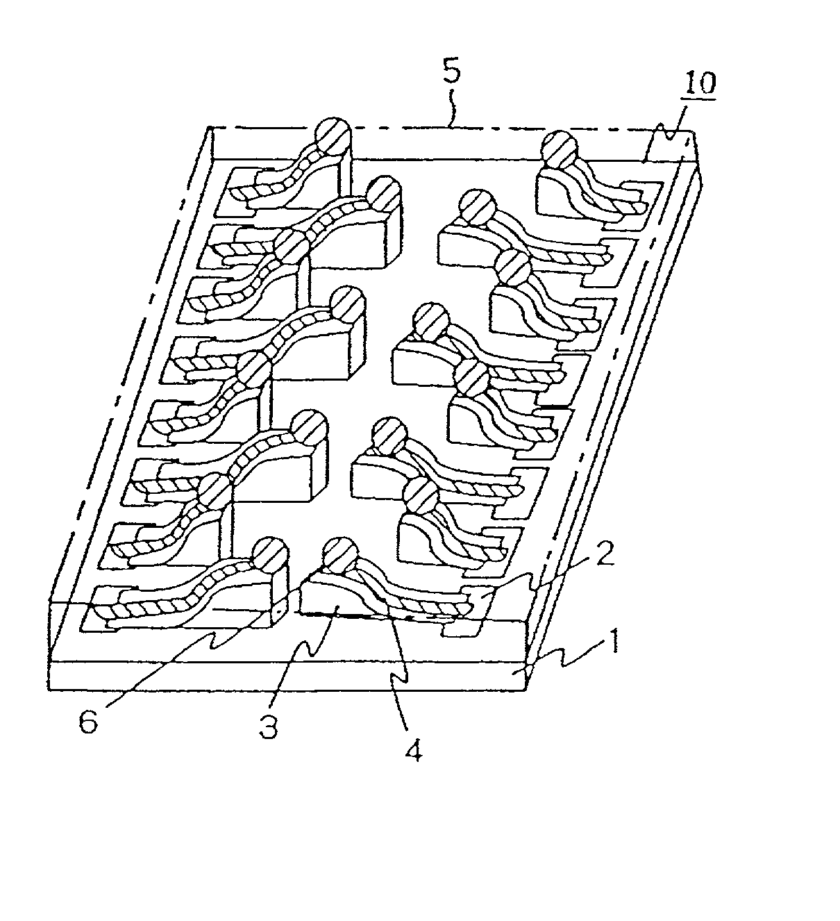
[0029] In the present specification, the wording "semiconductor element arranged to form integrated circuitry" may refer to an integrated circuit having at least one built-in circuit including a memory, logic, and microcomputer or else-practically, such as an LSI, VLSI, ULSI or other similar highly integrated ICs. In such a semiconductor element, one or more electrode pads for use as input / output terminal regions capable of inputting and outputting signals from and to external circuitry are formed so as to be electrically connected to a circuit section on the integrated circuit formation side. Further, in accordance with this invention, bump electrodes for external connection are formed so as to overlie the electrode pads with a conductive layer interposed therebetween. In accordance with this invention, it is required that more than one conductor section be formed on or over an insulative or di...


PUM


Abstract

A semiconductor device and a manufacturing method thereof, which device includes a semiconductor element arranged to form integrated circuitry, a plurality of electrode pads formed on the side of the integrated circuitry formation surface of the semiconductor element, bump electrodes for electrically connecting to the electrode pads through a conductive layer, and a stress relaxation layer formed between the integrated circuitry formation surface and electrode pads on one hand and the bump electrodes and conductive layer on the other hand, the stress relaxation layer being adhered thereto, wherein more than one third of the stress relaxation layer from a surface thereof is cut away for removal and wherein the stress relaxation layer is subdivided into a plurality of regions. Accordingly, it is possible to provide a semiconductor device capable of offering high density mounting schemes with increased reliability while reducing production costs.

Description

BACKGROUND OF THE INVENTION[0001] The present invention relates generally to semiconductor devices as well as semiconductor modules; and, more particularly, the invention relates to architectures or techniques for fabricating semiconductor elements in a form capable of being mounted in units of wafers and for subdividing this into necessary sizes to thereby obtain the intended semiconductor devices.[0002] In recent years, as electrical and electronic parts or components are increasing more and more in performance, semiconductor elements have likewise increased in integration density and functionality in a way such that the IC complexity has advanced from large-scale integration (LSI) to very-large-scale integration (VLSI), and finally to ultralarge-scale integration (ULSI). Such technological growth results in further increases in dimension and pin number, plus the operating rate of the elements involved. To accommodate this technical trend, package structures for use with multiple-...

Claims


Application Information

Patent Timeline
Patent Type & Authority Applications(United States)
IPC IPC(8): H01L21/60H01L23/31H01L23/485
CPCH01L23/3114H01L24/16H01L2224/0231H01L2224/13099H01L2924/01029H01L2924/01039H01L2924/01078H01L2924/01079H01L2924/01082H01L2924/14H01L2924/30107H01L2924/01005H01L2924/01006H01L2924/01033H01L2924/014H01L2224/0401H01L2924/351H01L2924/00H01L2924/12042H01L2224/0236H01L24/03H01L24/05H01L24/08H01L24/13H01L2224/02145H01L2224/02377H01L2224/08225H01L2924/01004H01L2924/01013H01L2924/01015H01L2924/01027H01L2924/01057H01L2924/01074
Inventor NAGAI, AKIRAUENO, TAKUMIAKAHOSHI, HARUOEGUCHI, SYUJIOGINO, MASAHIKOSATOH, TOSHIYANISHIMURA, ASAOANJOH, ICHIRO
Owner RENESAS ELECTRONICS CORP
Why Eureka
Try Eureka