

Semiconductor device
a technology of semiconductor devices and semiconductors, applied in the direction of semiconductor devices, semiconductor/solid-state device details, electrical apparatus, etc., can solve the problems of low em resistance in conventional semiconductor devices, crack resistance, and wire breakage, and achieve the effect of improving em resistan
- Summary
- Abstract
- Description
- Claims
- Application Information
AI Technical Summary
Benefits of technology
Problems solved by technology
Method used
Image

Examples
first embodiment
[0038] (First Embodiment)
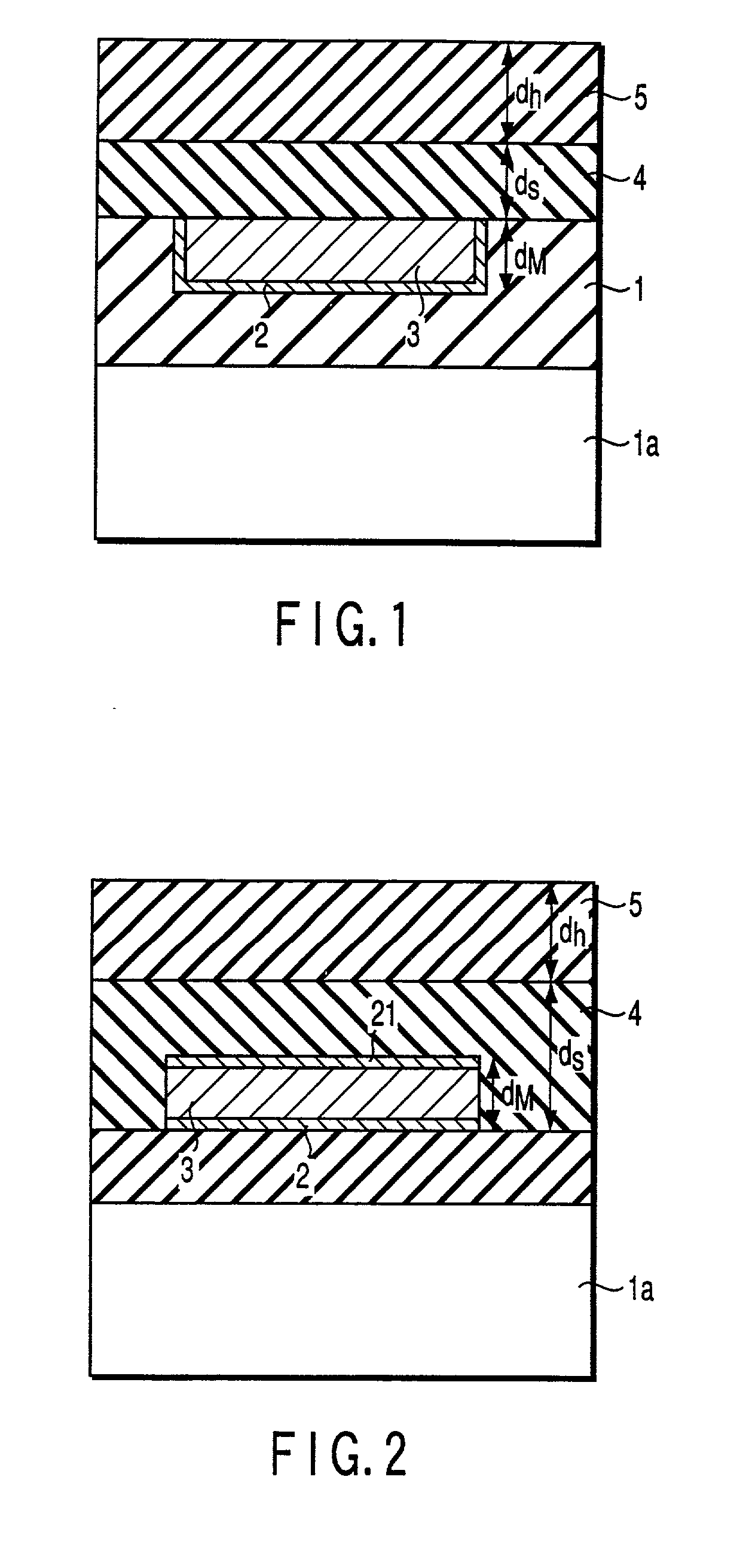
[0039] FIG. 1 is a cross sectional view of a semiconductor device according to a first embodiment of the present invention. In the present embodiment, an description will be made of a case where an insulation film having a Young's modulus of 15 GPa or lower is formed on the upper surface of a wiring in contact with the wiring.
[0040] As shown in FIG. 1, a trench of a thickness of 400 nm is formed on a TEOS-SiO.sub.2 film 1 on a substrate 1a. Within this trench, a wiring 3 is formed via a liner material 2. A transistor or the like (not shown), for example, is formed on the substrate 1a. The wiring 3 is brought into contact with, for example, a diffusion layer or the like (not shown) that structures this transistor, via the liner material 2. In this case, the wiring 3 is applied for lower layer, but it can also be applied for upper layer, and the substrate 1a can be used as compound semiconductor substrate or LCD substrate. This also applies to the following de...
second embodiment
[0069] (Second Embodiment)
[0070] FIG. 2 is a cross sectional view of a semiconductor device according to a second embodiment of the present invention. In the present embodiment, an description will be made of a case where an insulation film having a Young's modulus of 15 GPa or lower is formed on an upper surface and side surfaces of a wiring in contact with the wiring. In the following embodiment, structural parts common to those of the first embodiment are attached with identical reference symbols, and their detailed description will be omitted.
[0071] As shown in FIG. 2, a wiring 3 is formed on a TEOS-SiO.sub.2 film 1 on a substrate 1a. A first insulation film 4 is formed on the whole surface of the TEOS-SiO.sub.2 film 1 so that the first insulation film 4 is in contact with the upper surface and the side surfaces of the wiring 3. A second insulation film 5 is formed on the first insulation film 4. A liner material 2 is formed between the wiring 3 and the TEOS-SiO.sub.2 film 1. Al...
third embodiment
[0084] (Third Embodiment)
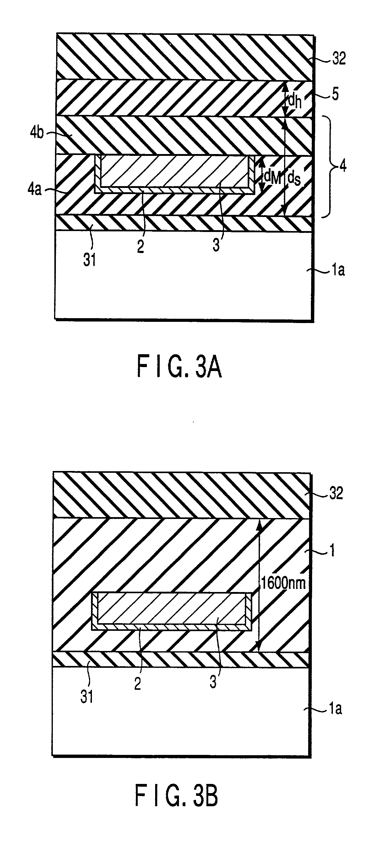
[0085] FIG. 3A is a cross sectional view of a semiconductor device according to a third embodiment of the present invention. In the present embodiment, an description will be made of a case where the whole surfaces of a wiring are surrounded by an insulation film having a Young's modulus of 15 GPa or lower.
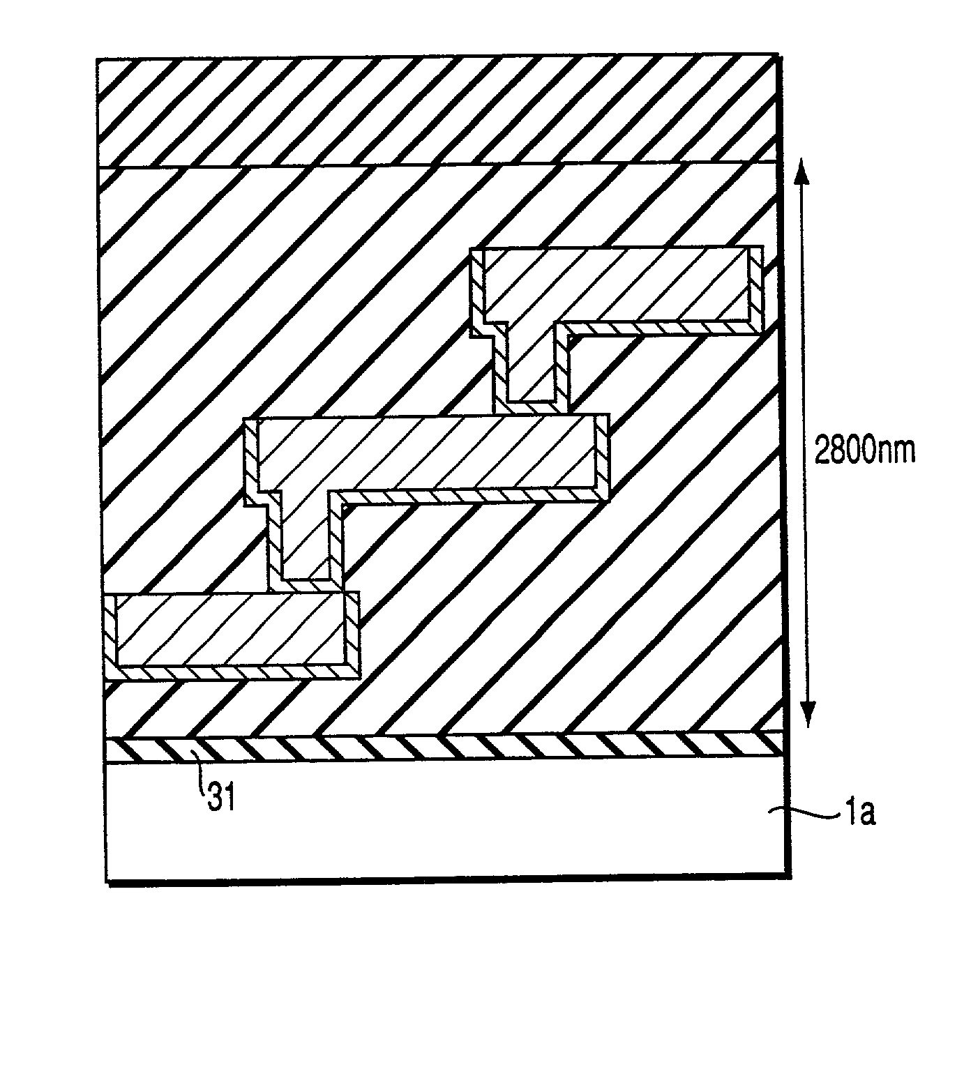
[0086] As shown in FIG. 3A, a first insulation film 4 is formed on a thermally-oxidized SiO.sub.2 film 31 on a substrate 1a. The first insulation film 4 has a laminated structure of interlayer insulation films 4a and 4b. The interlayer insulation film 4a is formed with a trench. A liner material 2 is formed to cover a 4 bottom surface and side surfaces of this trench. A wiring 3 is embedded into this trench via the liner material 2. A second insulation film 5 is formed on the first insulation film 4. Further, a plasma SiN film 32 is formed on the second insulation film 5. The first insulation film 4 is made of a material having a Young's modulus of 15 GPa ...
PUM
 Abstract
Description
Claims
Application Information