Semiconductor device and method for manufacturing same

a technology of semiconductors and semiconductors, applied in the direction of semiconductor/solid-state device details, water-setting substance layered products, coatings, etc., can solve the problem of limiting the operating speed of electronic elements, simultaneous enhancement of both resistances cannot be achieved in conventional technologies, simultaneous enhancement of both resistances cannot be achieved, etc., to achieve enhanced siv resistance, improve siv resistance, and reduce carbon concentration

Active Publication Date: 2007-08-16
RENESAS ELECTRONICS CORP
View PDF2 Cites 13 Cited by
  • Summary
  • Abstract
  • Description
  • Claims
  • Application Information

AI Technical Summary

Benefits of technology

[0019]A present inventors have made an attempt on achieving simultaneous improvements in both of the SIV resistance and the EM resistance, which are in a relationship of a trade-off, and thus a procedure for manufacturing the copper-containing metallic film of the semiconductor device has been investigated in various ways. As a result of the investigations, the inventors have found that the semiconductor device, which is configured that the distribution of carbon concentration along the depositing direction in the copper-containing electrically conducting film includes the first peak and the second peak, can be obtained by the above-described manufacturing process. It can be achieved by conducting such process that peaks in the carbon concentration appear at positions that are closer to the interface of the copper-containing electrically conducting film and the barrier metal film, thereby providing further improved SIV resistance. Further, a reduced carbon concentration in interface between the copper-containing electrically conducting film and the barrier metal film can be maintained, so that an enhanced SIV resistance can be provided without deteriorating the EM resistance. Further, a relatively higher carbon concentration between the first peak and the second peak can be maintained, thereby providing an enhanced SIV resistance. Further, by conducting such method, a continuously uniform two-dimensional carbon concentration profile in the copper-containing electrically conducting film formed on the barrier metal film can be obtained along the barrier metal film. This configuration provides an improved adhesiveness between the copper-containing electrically conducting film and the barrier metal film in both the bottom surface and the side surface of the copper-containing electrically conducting film, thereby providing an enhanced EM resistance. Further, further improved SIV resistance can also be provided.
[0020]According to the present invention, an improved SIV resistance and an improved EM resistance can be achieved in the coupling structure containing copper films.

Problems solved by technology

In semiconductor devices of recent years, a delay in signal propagation through an interconnect restricts an operating speed of electronic elements.
As described above, an improvement in SIV resistance and an improvement in EM resistance is a trade off, and thus simultaneous enhancements of both resistances can not be achieved in conventional technologies.
In the configurations described in above-described conventional technologies, simultaneous improvements in both SIV resistance and EM resistance can not be achieved.

Method used


Image

  • Semiconductor device and method for manufacturing same
  • Semiconductor device and method for manufacturing same
  • Semiconductor device and method for manufacturing same

Examples


example 1

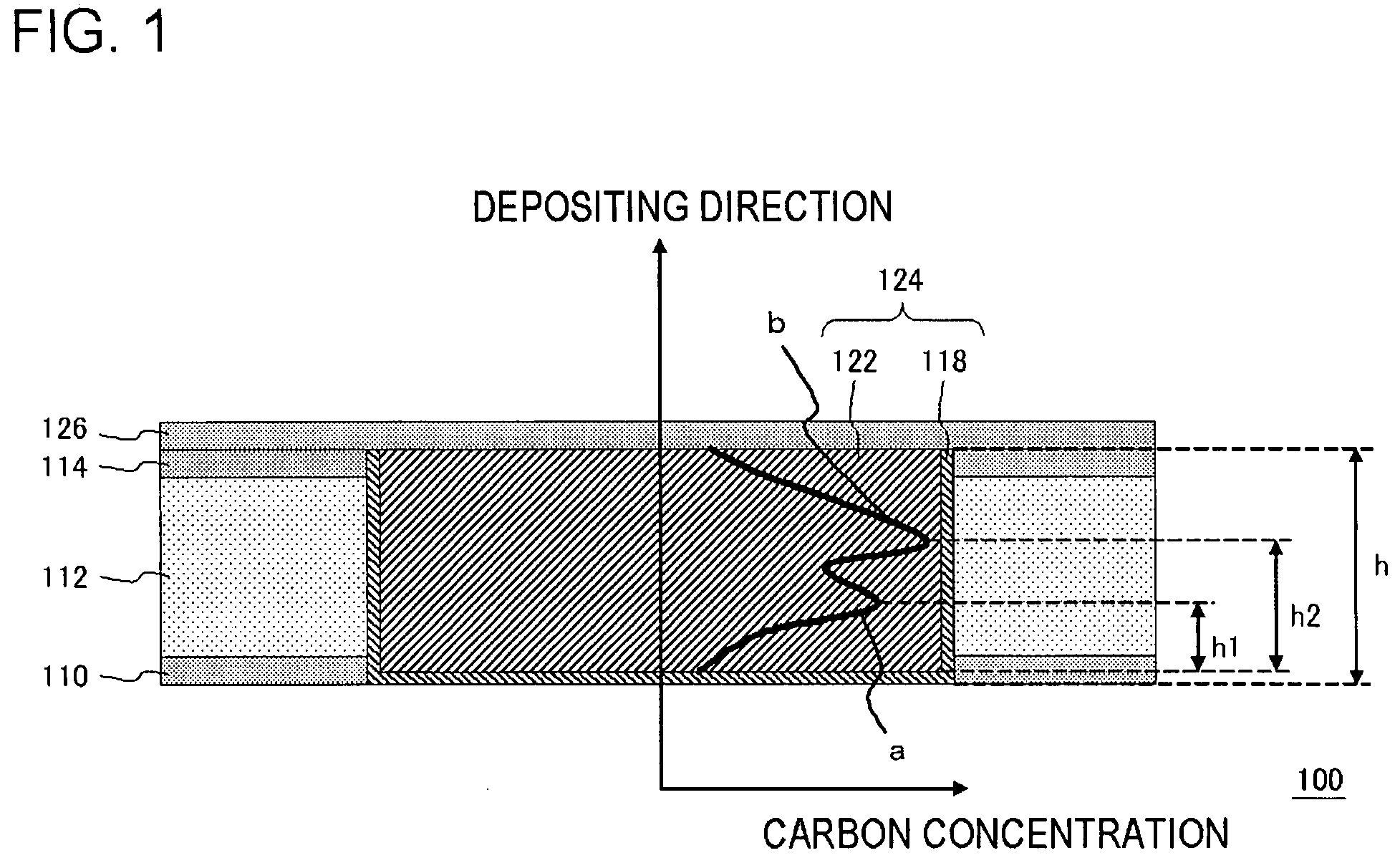
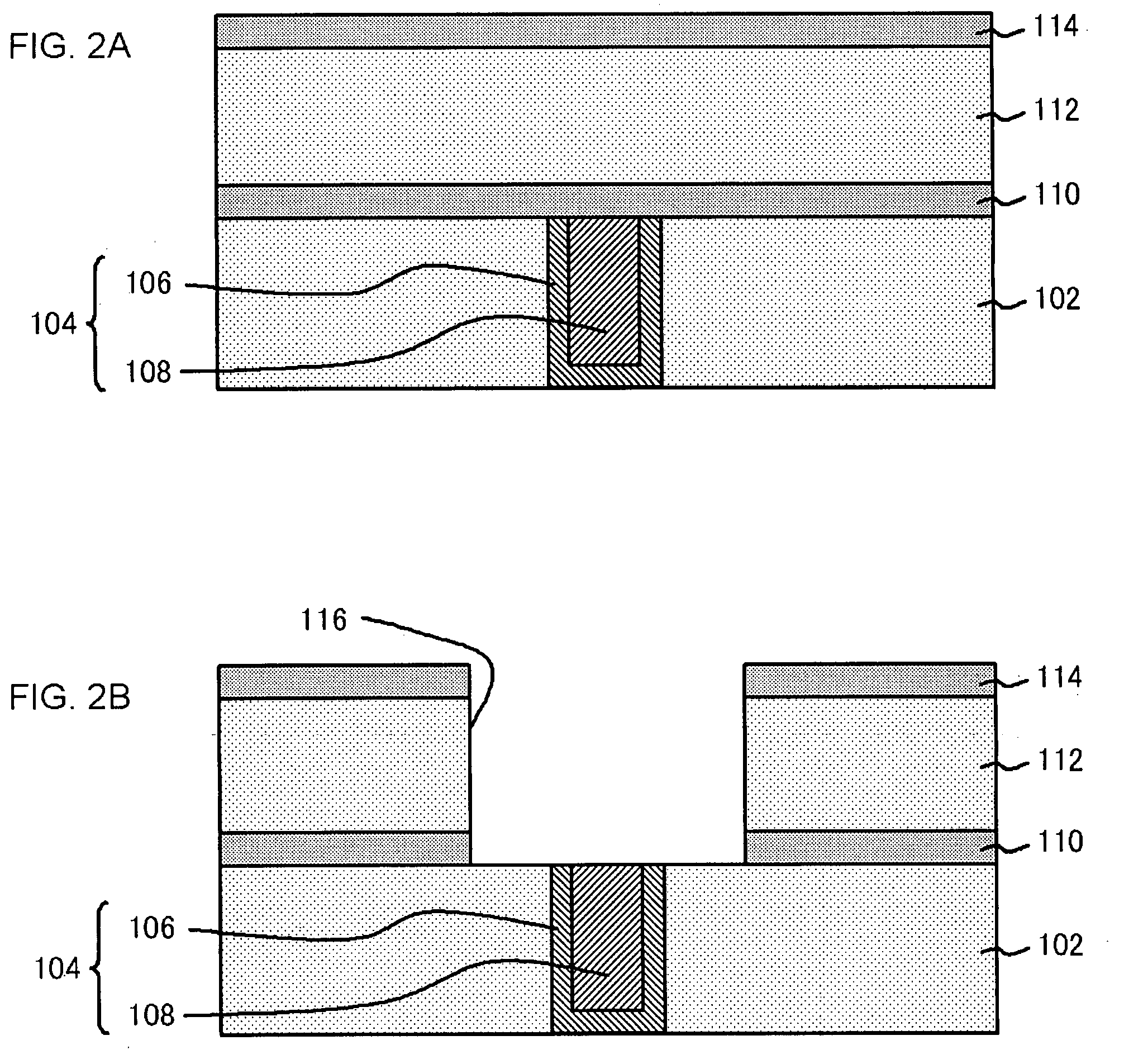
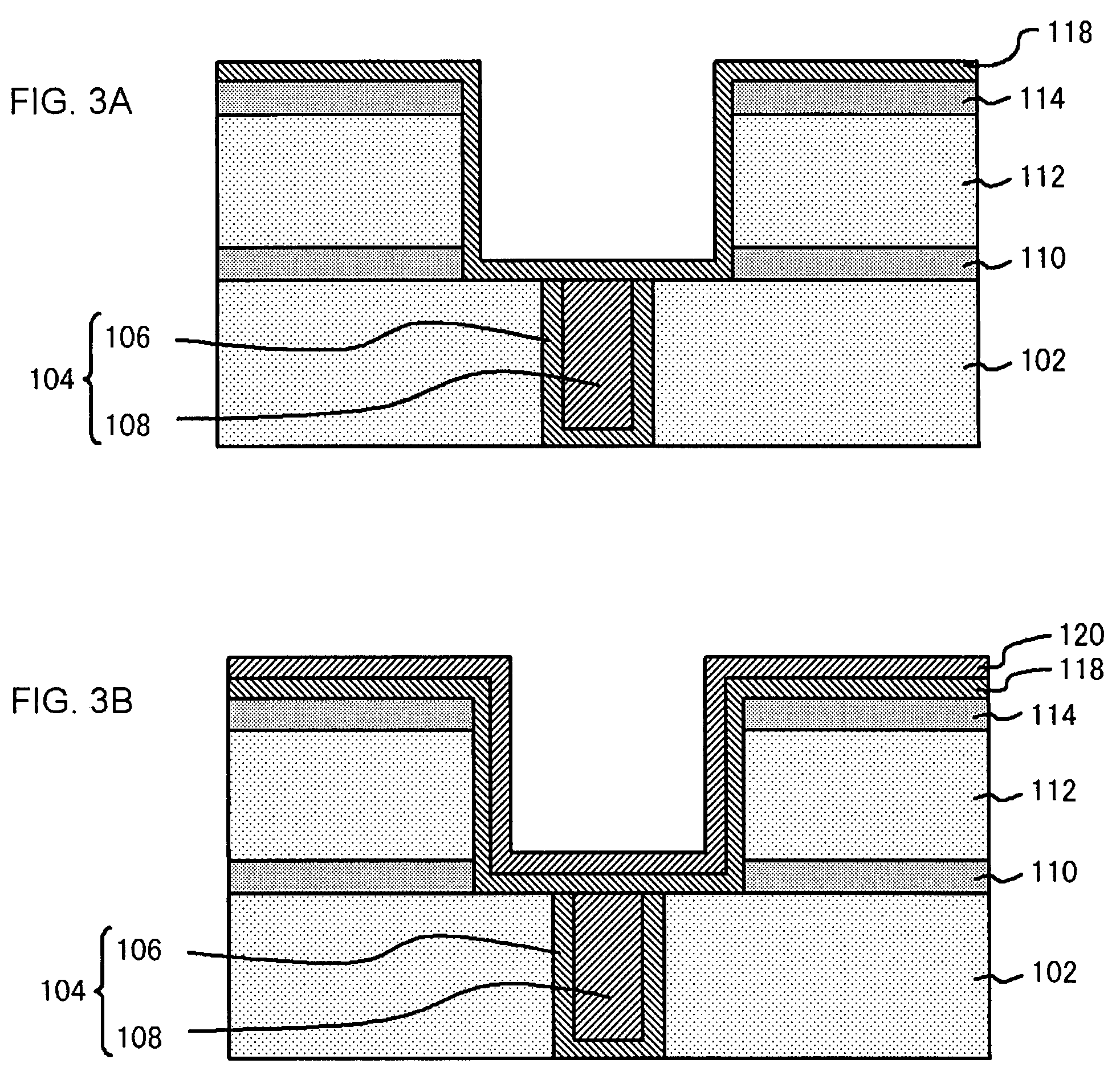
[0059]The second barrier metal film 118 was configured to be formed by depositing a TaN film (film thickness of about 5 nm) and a Ta film (film thickness of about 10 nm) in this order. The seed metallic film 120 was composed of an alloy of copper and Al (Al content of 1 atomic %, film thickness of about 50 nm). The employed plating solution contained polyethylene glycol of molecular weight within a range equal to or more than 500 to equal to or less than 2,000. Further, the plating solution was also designed to contain copper at a concentration of 50 g / liter. The semiconductor substrate was placed in a bath containing such plating solution, and a current density at the time of placing the semiconductor substrate in the bath was set to be within a range equal to or more than 3 mA / cm2 to less than 8 mA / cm2. Further, after trenches in a fine pattern had been filled (about 2 minutes passed after placing the substrate into the bath), the current density was increased to a level of within...

example 2

[0062]The present example was similarly performed as in example 1, except that the employed plating solution contained polyethylene glycol and polypropylene glycol of molecular weight within a range equal to or more than 500 to equal to or less than 2,000. Except for such formulation of the plating solution, the semiconductor device 100 was manufactured similarly as example 1. Thermal processing operations were performed under three conditions of: (i) within a hydrogen containing nitrogen atmosphere (hydrogen concentration of 4% vol.) at about 250 degree C. for about 30 seconds; (ii) within a hydrogen containing nitrogen atmosphere (hydrogen concentration of 4% vol.) at about 350 degree C. for about 30 seconds; and (iii) within a nitrogen atmosphere at about 250 degree C. for about 30 minutes, similar as in example 1. These results are respectively shown in FIG. 6A to FIG. 6C. In each of these charts, a vertical dotted line indicates the interface between the seed metallic film 120 ...


PUM

PropertyMeasurementUnit
heightaaaaaaaaaa
heightaaaaaaaaaa
heightaaaaaaaaaa

Abstract

An improved SIV resistance and an improved EM resistance are achieved in the coupling structure containing copper films. A semiconductor device includes: a semiconductor substrate; a second insulating layer formed on or over the semiconductor substrate; a second barrier metal film, formed on the second insulating film, and being capable of preventing copper from diffusing into the second insulating film; and an electrically conducting film formed on the second barrier metal film so as to be in contact with the second barrier metal film, and containing copper and carbon, wherein a distribution of carbon concentration along a depositing direction in the second electrically conducting film includes a first peak and a second peak.

Description

[0001]This application is based on Japanese patent application No. 2006-36,921, the content of which is incorporated hereinto by reference.BACKGROUND[0002]1. Technical Field[0003]The present invention relates to a semiconductor device and a method for manufacturing thereof.[0004]2. Related Art[0005]In semiconductor devices of recent years, a delay in signal propagation through an interconnect restricts an operating speed of electronic elements. A delay constant in signal propagation through an interconnect is represented by a product of an interconnect resistance and an interconnect capacitance. Therefore, in order to achieve faster operation of elements, a low dielectric constant material having lower dielectric constant than a conventional silicon dioxide film (SiO2) is employed for an interlayer insulating film, and copper (Cu) having lower electrical resistivity is employed for an interconnect.[0006]A multiple-layered interconnect employing copper as an interconnect material is ...

Claims


Application Information

Patent Timeline
Patent Type & Authority Applications(United States)
IPC IPC(8): C25D5/02B32B13/04
CPCC25D3/38C25D5/50C25D15/00H01L21/2885C25D7/123H01L21/76829H01L21/76873H01L21/76877H01L21/76883H01L21/76801
Inventor FURUYA, AKIRAARITA, KOJIKUROKAWA, TETSUYANODA, KAORI
Owner RENESAS ELECTRONICS CORP
Why Eureka
Try Eureka