Semiconductor device having insulating film with surface modification layer and method for manufacturing the same

a technology of insulating film and semiconductor device, which is applied in the direction of semiconductor device, semiconductor/solid-state device details, electrical apparatus, etc., can solve the problems of film peeling or generation of particles or watermarks, low mechanical strength and hydrophobic surface of low dielectric constant film, and the inability to achieve the effect of reducing the generation of watermarks in the cmp process

Inactive Publication Date: 2010-03-11
RENESAS ELECTRONICS CORP
View PDF5 Cites 14 Cited by
  • Summary
  • Abstract
  • Description
  • Claims
  • Application Information

AI Technical Summary

Benefits of technology

[0032]According to the manufacturing method for the semiconductor device, the surface modification layer is formed by the plasma treatment using the inert gas performed on the surface layer of the SiOCH film, and therefore is thinner than the case of depositing the film. Therefore, even if a dielectric constant of the surface modification layer is higher than a dielectric constant of the SiOCH film, it is possible to suppress an increase in the dielectric constant of the entire SiOCH film because the surface modification layer is sufficiently thin.
[0033]Moreover, the surface modification layer has the lower carbon concentration and the higher oxygen concentration than the first insulating film has, and thus has an affinity for water. Therefore, sweat hardly remains on the surface modification layer that is exposed in the CMP process, and hence residual particles and generation of a watermark of ter the CMP process can be reduced.
[0034]According to the present invention, it is possible to realize the semiconductor device having the structure in which the interlayer insulating film made of a low dielectric constant film can be protected from damage in the CMP process, and an effective dielectric constant of the interlayer insulating film is reduced, and the manufacturing method for the semiconductor device.

Problems solved by technology

In a case of forming Cu wirings, a dry etching process is difficult, and hence a damascene method is used in most cases.
However, the low dielectric constant film has characteristics of low mechanical strength and a hydrophobic surface.
Therefore, if the low dielectric constant film is exposed in the CMP process for forming the Cu wirings by the damascene method, there may be a problem of film peeling or generation of particles or a watermark due to detergent deterioration.

Method used


Image

  • Semiconductor device having insulating film with surface modification layer and method for manufacturing the same
  • Semiconductor device having insulating film with surface modification layer and method for manufacturing the same
  • Semiconductor device having insulating film with surface modification layer and method for manufacturing the same

Examples


first embodiment

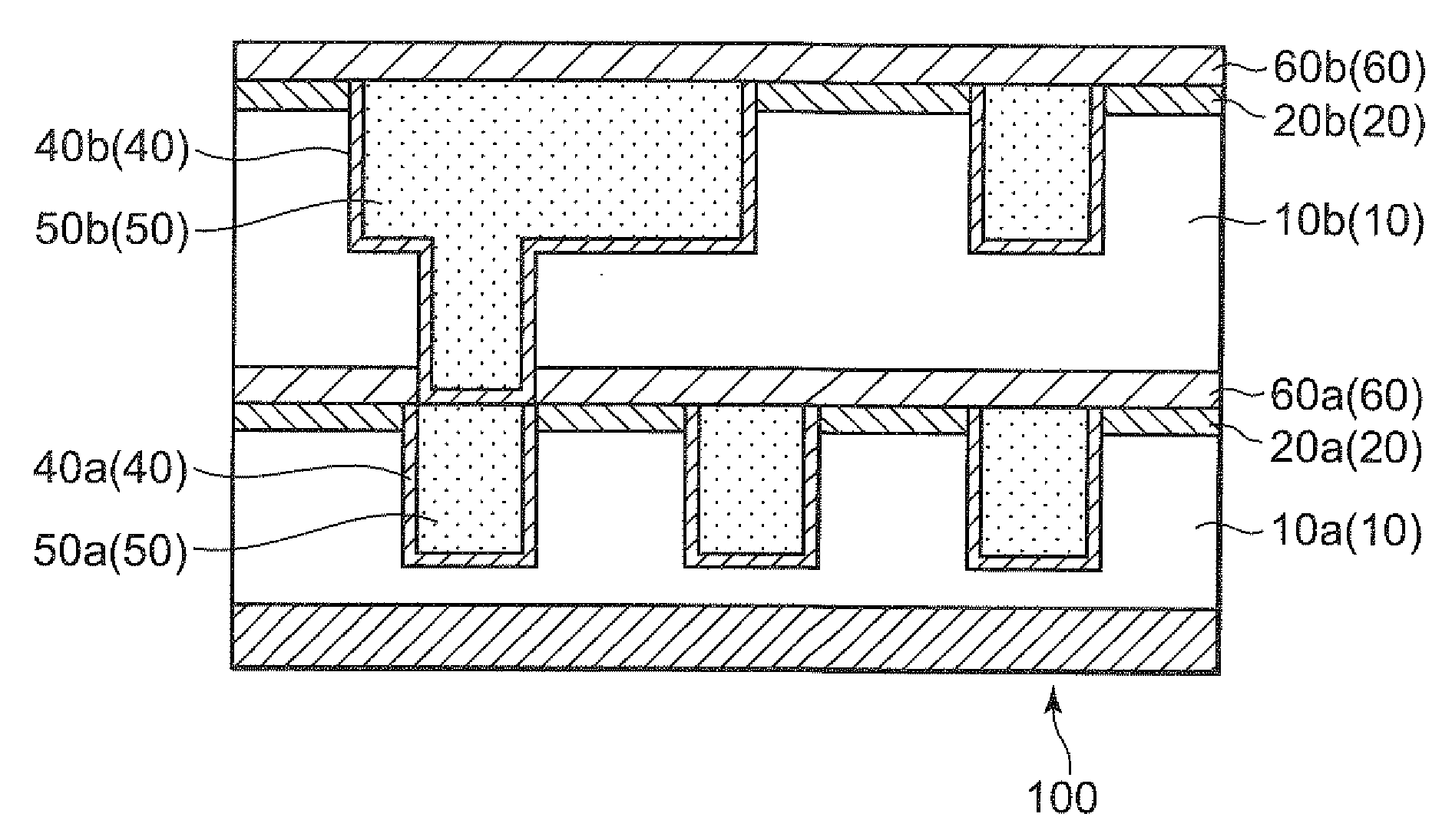
[0055]FIG. 1 is a cross section illustrating a semiconductor device according to a first embodiment of the present invention.

[0056]A semiconductor device 100 includes:

[0057]a semiconductor substrate;

[0058]an SiOCH film 10 (first insulating film) formed on the semiconductor substrate;

[0059]a surface modification layer 20 including an SiOCH film formed by modifying a surface layer of the SiOCH film 10, the SiOCH film having a lower carbon concentration and a higher oxygen concentration than the SiOCH film 10 has;

[0060]a Cu wiring 50 filled in a recess formed in the surface modification layer 20 and the SiOCH film 10; and

[0061]a cap insulating film (second insulating film) 60 contacting surfaces of the Cu wiring 50 and the surface modification layer 20.

[0062]The SiOCH film 10 (10a and 10b) is formed on the semiconductor substrate. The SiOCH film 10 works as a film for reducing capacitance between multilayer wires for connecting semiconductor elements.

[0063]The SiOCH film 10 is a low di...

example 1

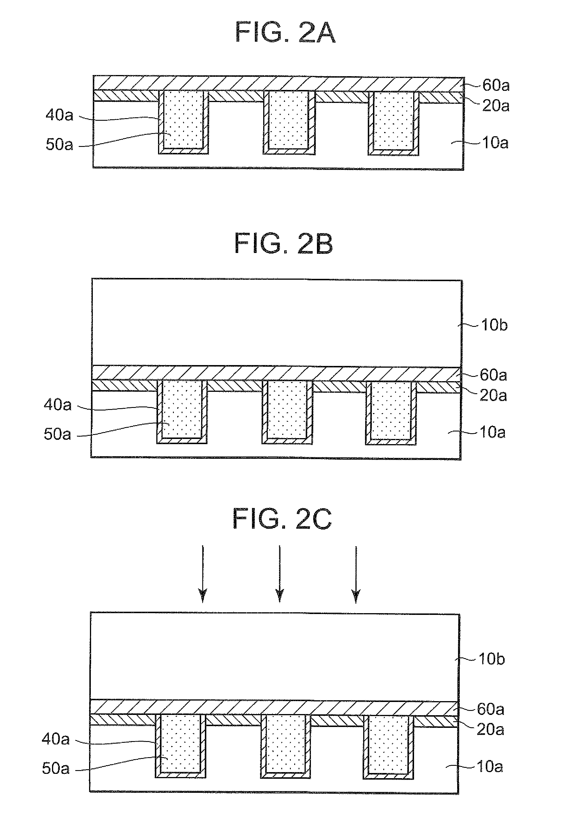
[0124]First, the SiO2 film having a thickness of 300 nm was formed on the silicon substrate, and the first wiring layer was formed on the same by the single damascene method.

[0125]Next, the porous SiOCH film was formed on the SiO2 film by the plasma CVD method using the raw material having the cyclic organic silica structure expressed in the following Formula (3) in the same manner as described above in the first embodiment. The porous SiOCH film is the insulating film between wires, and its thickness was 120 nm while the relative dielectric constant was 2.5.

[0126]After that, the He plasma treatment was performed at the RF power of 440 W for 15 seconds of the process time, and hence the surface modification layer was formed on the surface of the porous SiOCH film.

[0127]Further on the surface modification layer, the SiO2 film having a thickness of 80 nm was formed as the hard mask by the plasma CVD method using SiH4 gas as a source gas in the same chamber as the He plasma treatment c...


PUM


Abstract

Provided is a semiconductor device, which includes an interlayer insulating film formed on a semiconductor substrate, a wiring layer filled in a recess formed in the interlayer insulating film, and a cap insulating film. The interlayer insulating film includes a first SiOCH film and a surface modification layer including an SiOCH film formed by modifying a surface layer of the first SiOCH film, the SiOCH film having a lower carbon concentration and a higher oxygen concentration than the first SiOCH film has. The cap insulating film contacts with surfaces of the metal wiring and the surface modification layer.

Description

BACKGROUND OF THE INVENTION[0001]1. Field of the Invention[0002]The present invention relates to a semiconductor device and a manufacturing method for the semiconductor device.[0003]2. Description of the Related Art[0004]Conventionally, aluminum (Al) or an aluminum alloy is widely used as a material for wirings of a semiconductor device, while a silicon oxide (SiO2) film is widely used as a material for an interlayer insulating film of the semiconductor device. However, along with a progress in a finer pattern and higher speed of semiconductor devices, for improving a signal transmission delay in wirings, copper (Cu) having a lower resistance has become to be used as the material for wirings, whereas low dielectric constant film having lower dielectric constant such as an SiOCH film has become to be used as the insulating film.[0005]In a case of forming Cu wirings, a dry etching process is difficult, and hence a damascene method is used in most cases. The damascene method includes s...

Claims


Application Information

Patent Timeline
Patent Type & Authority Applications(United States)
IPC IPC(8): H01L23/532H01L23/522H01L21/768
CPCH01L21/02126H01L21/02203H01L2924/0002H01L21/02216H01L21/02274H01L21/0234H01L21/3105H01L21/31633H01L21/31695H01L21/7682H01L21/76826H01L21/76829H01L21/76832H01L23/5222H01L23/53238H01L23/5329H01L23/53295H01L2221/1047H01L2924/00
Inventor UEKI, MAKOTOONODERA, TAKAHIROHAYASHI, YOSHIHIRO
Owner RENESAS ELECTRONICS CORP
Why Eureka
Try Eureka