

Metal film decarbonizing method, film forming method and semiconductor device manufacturing method
a metal-based film and film forming technology, applied in the direction of solid-state diffusion coating, chemical vapor deposition coating, coating, etc., can solve the problems of deterioration of electrical characteristics of the depletion layer formed at the interface between a poly-si film and an underlying gate oxide film, the need for high integration and high speed of an lsi requires a decrease in the resistance of the gate electrode, etc., to achieve suppressed deterioration of the work
- Summary
- Abstract
- Description
- Claims
- Application Information
AI Technical Summary
Benefits of technology
Problems solved by technology
Method used
Image

Examples
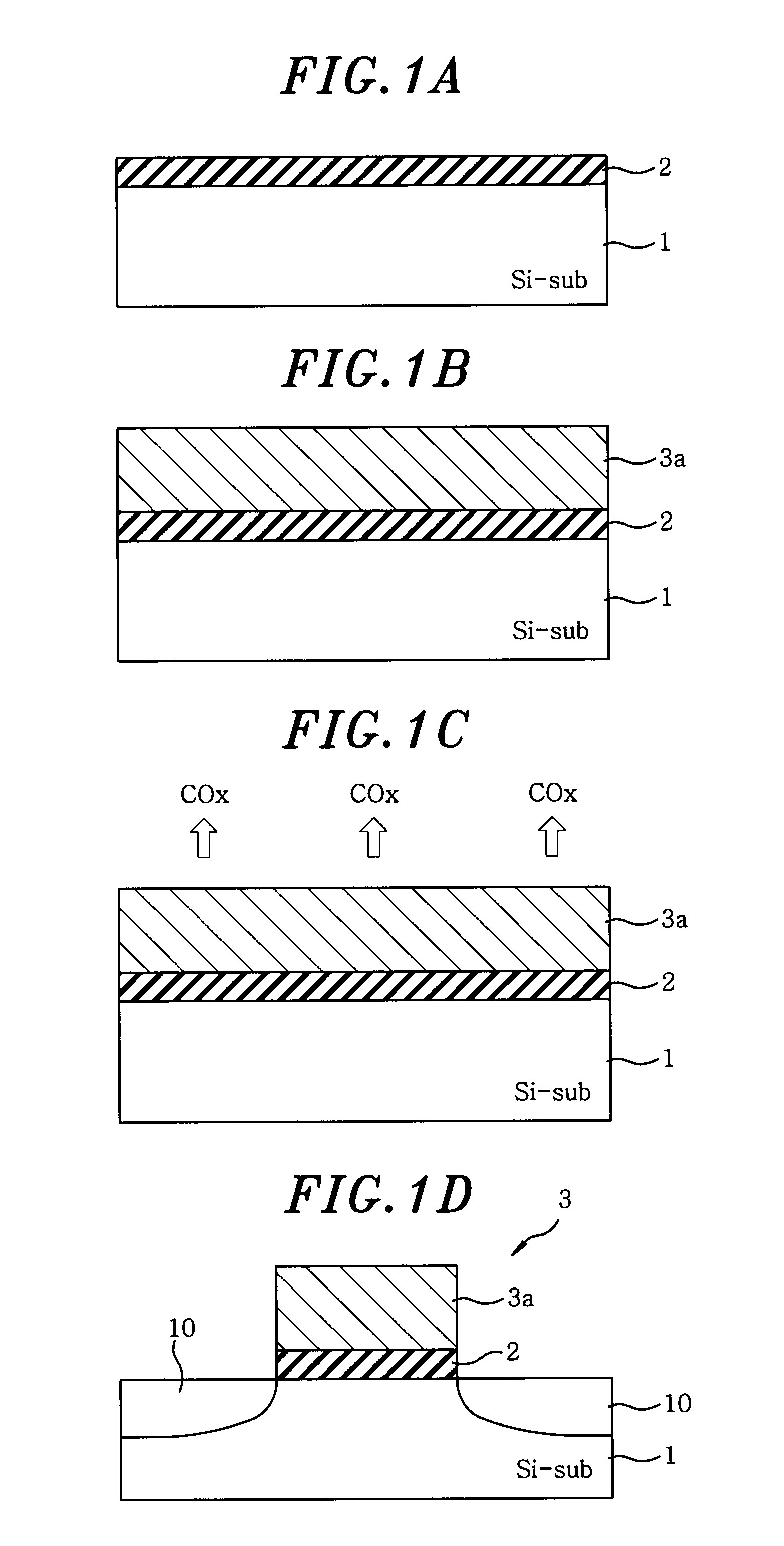
first embodiment
[0064]As for the first embodiment of the decarbonizing method of the present invention, there will be described a thermal oxidation process (selective oxidation) performed in an oxidizing atmosphere using an oxidizing agent under existence of a reducing gas. Here, as for a reducing gas, it is possible to use, e.g., H2, NH3 or the like. As for an oxidizing agent, it is possible to use, e.g., O2, water vapor (H2O), N2O, NO or the like.
[0065]The thermal oxidation process can be performed in the processing chamber of a diffusion furnace having a known configuration. Desired conditions of the thermal oxidation process will be described hereinafter.
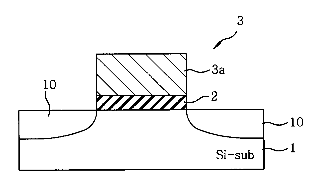
[0066]For example, it is preferable that a temperature of a wafer is lower than a conventional annealing temperature (1000° C.), e.g., about 650° C. to 940° C., more preferably, about 700° C. to 900° C. When the wafer temperature is higher than about 940° C., the W-based film 3a forming the gate electrode 3 or the gate insulating film 2 may be ...
second embodiment
[0071]Another embodiment of the decarbonizing method is a radical oxidation process using a plasma. The radical oxidation process can be performed in an oxidizing atmosphere using an oxidizing agent under existence of a reducing gas. The reducing gas and the oxidizing agent used in the first embodiment can be used in the second embodiment.
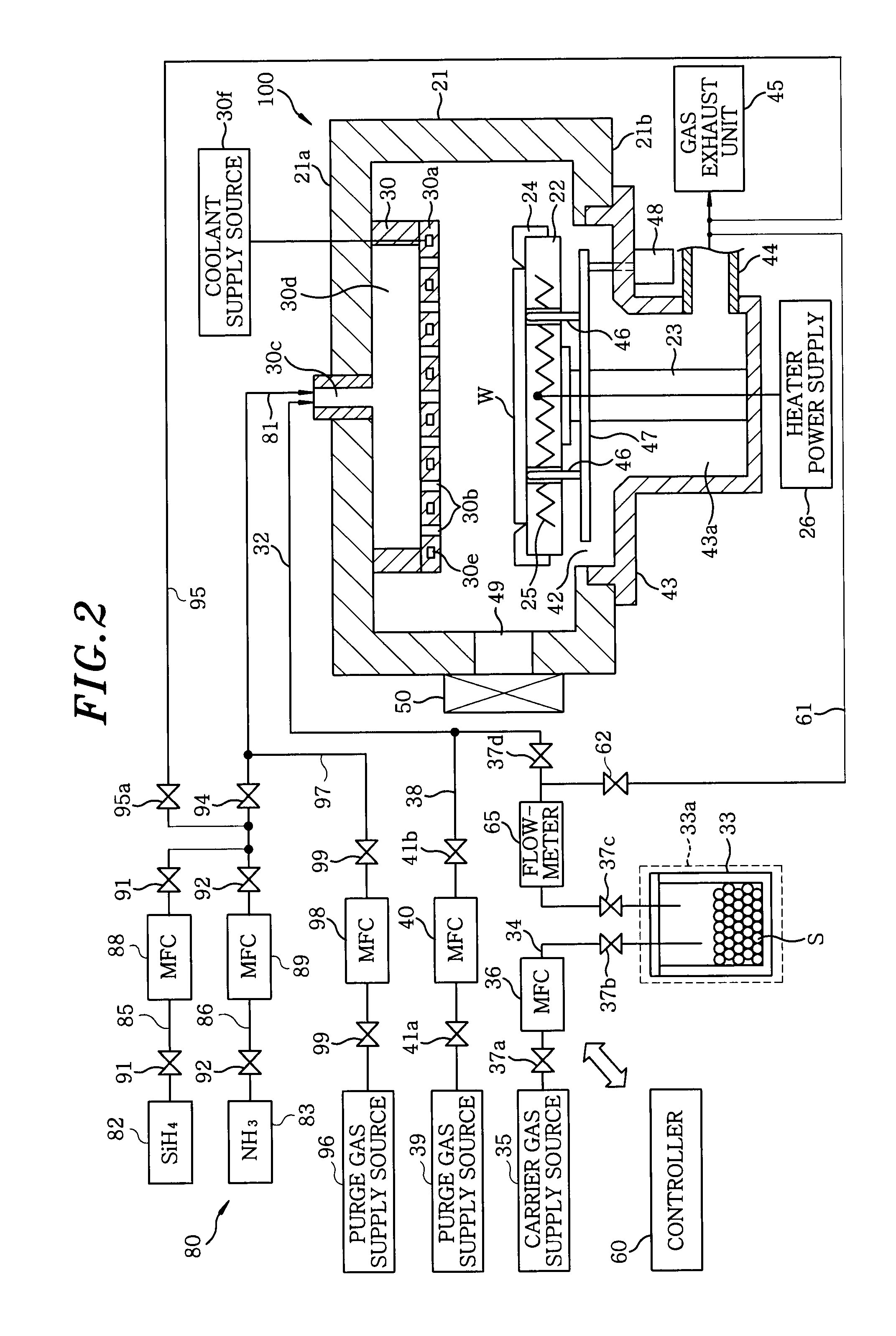
[0072]FIG. 3 offers a schematic cross sectional view of an example of a plasma processing apparatus applicable to the radical oxidation process as an example of the decarbonizing method. This plasma processing apparatus 200 is configured as a RLSA (radial line slot antenna) microwave plasma processing apparatus capable of generating a microwave-excited plasma of a high density and a low electron temperature by introducing microwaves into a processing chamber by using a planar antenna having a plurality of slots, particularly an RLSA. Therefore, this plasma processing apparatus 200 can perform a process using a plasma having a density of about 1011 ...
third embodiment
[0099]As for a third embodiment of the decarbonizing method of the present invention, there will be described a UV irradiation in an oxidizing atmosphere under existence of a reducing gas. The reducing gas and the oxidizing agent used in the first embodiment can be used in the third embodiment.
[0100]The UV irradiation can be performed in a processing chamber of a known UV irradiation apparatus having an UV lamp.
[0101]Hereinafter, desired conditions of the UV irradiation will be described. For example, it is preferable that the temperature of the wafer W is set to, e.g., about 250 to 600° C., more preferably, about 400 to 480° C. When the temperature of the wafer W is higher than about 600° C., the W-based film 3a forming the gate electrode 3 or the gate insulating film 2 may be oxidized. When the wafer temperature is lower than about 250° C., the decarbonization in the W-based film 3a may be insufficient.
[0102]Moreover, it is preferable that a pressure in a chamber (UV processing pr...
PUM
| Property | Measurement | Unit |
|---|---|---|
| pressure | aaaaa | aaaaa |
| temperature | aaaaa | aaaaa |
| pressure | aaaaa | aaaaa |
Abstract
Description
Claims
Application Information