CMOS structure with non-epitaxial raised source/drain and self-aligned gate and method of manufacture

Inactive Publication Date: 2002-10-03
IBM CORP
View PDF0 Cites 19 Cited by
  • Summary
  • Abstract
  • Description
  • Claims
  • Application Information

AI Technical Summary

Problems solved by technology

One key limitation of this method is that epitaxial growth must take place at temperatures as high as 750.degree. C., which causes significant transient enhanced diffusion (TED) of major dopants.
The unnecessary dopant redistribution in halo/extension regions degrades the performance of devices and short channel immunity.
Moreover, with a very thin SOI film, it can be difficult to form epitaxial silicon without causing silicon agglomeration due to possible contamination of carbon in certain chemical vapor deposition tools.
Howev

Method used


Image

  • CMOS structure with non-epitaxial raised source/drain and self-aligned gate and method of manufacture
  • CMOS structure with non-epitaxial raised source/drain and self-aligned gate and method of manufacture
  • CMOS structure with non-epitaxial raised source/drain and self-aligned gate and method of manufacture

Examples


Embodiment Construction

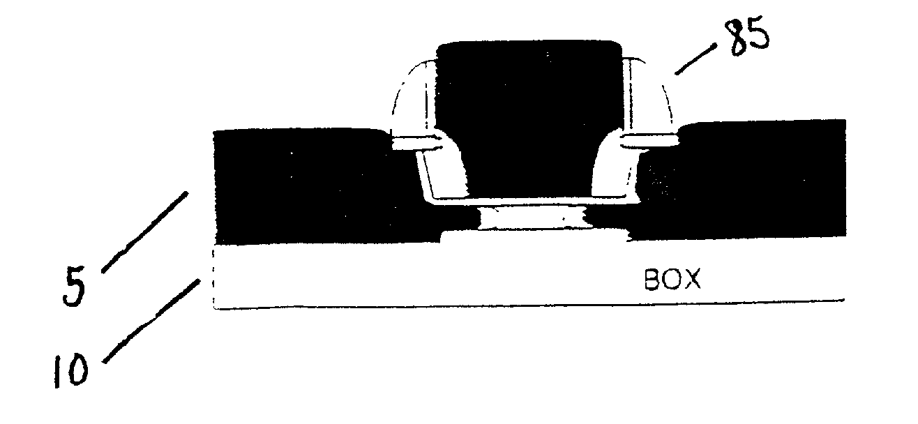
[0019] In the embodiments of the present invention, the CMOS structure is provided with a non-epitaxial raised source / drain and self-aligned gate. By using the method of the present invention, it is possible to form the CMOS structure with non-epitaxial raised source / drain.

Method of Formation of the Present Invention

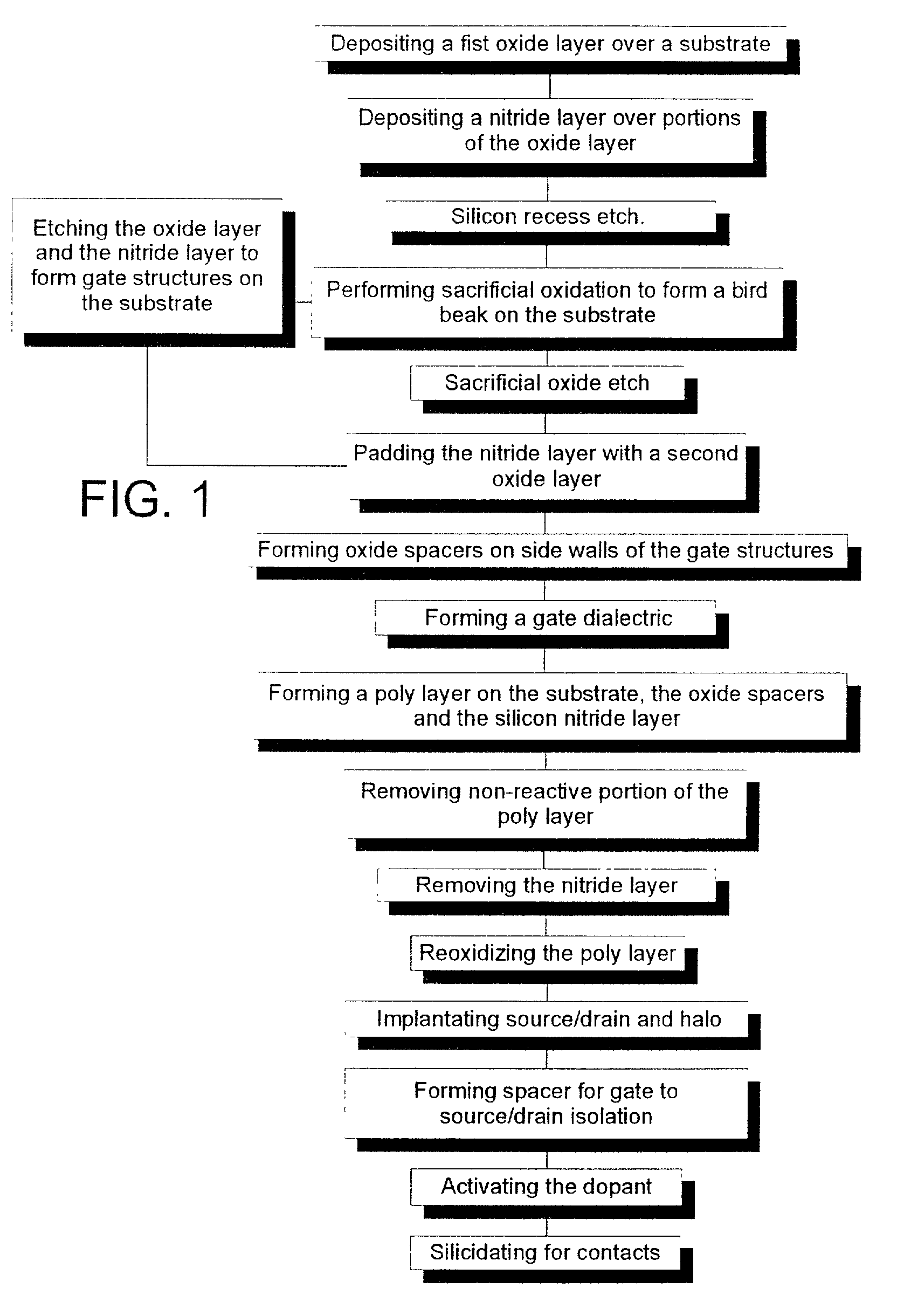
[0020] Referring now to the drawings, and more particularly to FIG. 1, there is shown a flow diagram of one exemplary embodiment of a fabrication process in accordance with the present invention. The fabrication process shown in FIG. 1 describes several embodiments, none of which are necessarily required in any one preferred embodiment but which still may be part of the present invention.

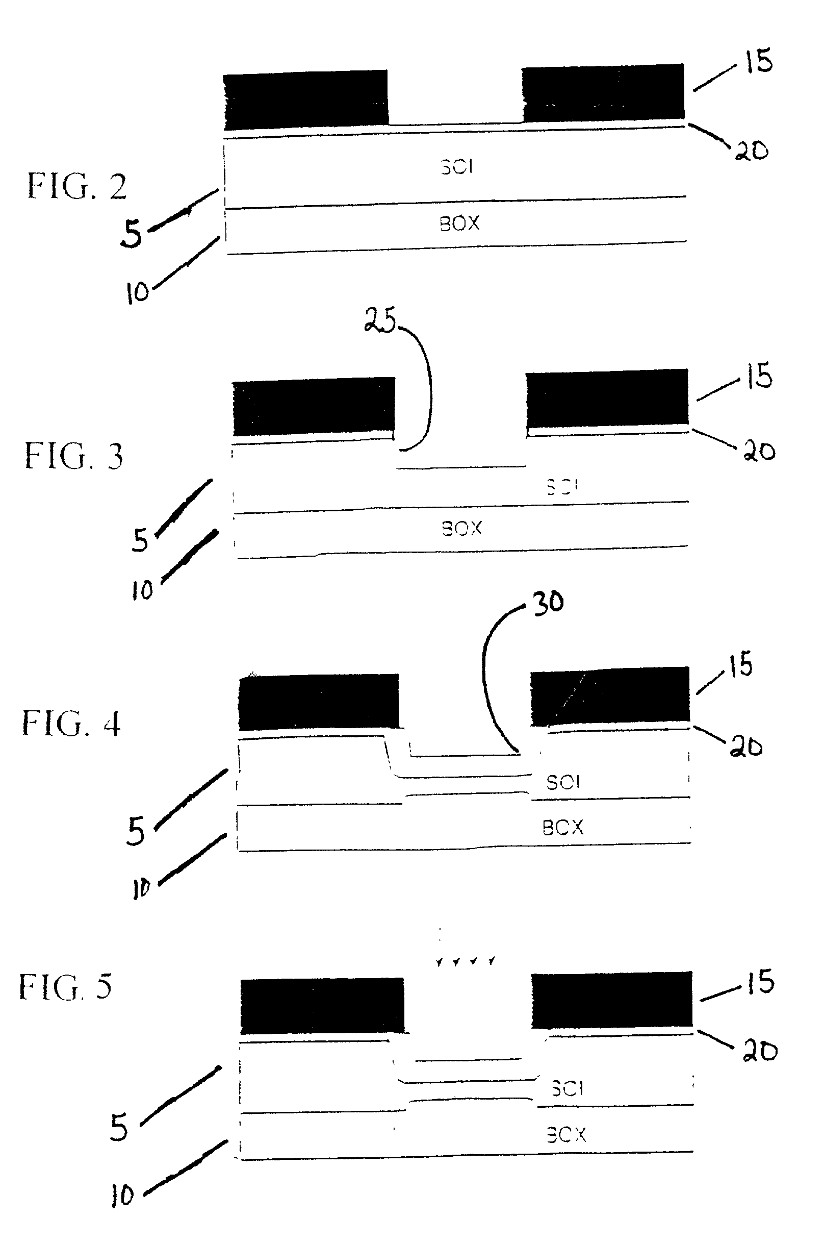
[0021] In process steps 100-200, an oxide and a nitride layer are deposited. See FIG. 2. The oxide is for buffering the stress from the nitride layer and also for etch stop. The thickness of nitride can be adjusted to match the final poly gate thickness and mask for poly gate definition....


PUM


Abstract

A CMOS structure and method of achieving self-aligned raised source/drain for CMOS structures on SOI without relying on selective epitaxial growth of silicon. In the method, CMOS structures are provided by performing sacraficial oxidation so that oxidation occurs on the surface of both the SOI and BOX interface. This allows for oxide spacer formation for gate-to-source/drain isolation which makes raised source/drain fabrication without increasing contact resistance possible.

Description

[0001] 1. Field of the Invention[0002] The present invention generally relates to CMOS structures and, more particularly, to a method of achieving high performance self-aligned low-resistance raised source / drain for CMOS on SOI, through differential thickness of source / drain and channel, without relying on selective epitaxial growth of silicon.[0003] 2. Background Description[0004] Complementary Metal Oxide Semiconductors (CMOS) are electronic components used for Random Access Memory (RAM) and fast data switching. CMOS semiconductors are made of two complementary metal-oxide field effect transistors for high speed and low power use. While many designs have been developed, Silicon On Insulator has recently been of interest due to the high capacity of silicon for high-performance structure fabrication having the channel controllable with low gate voltages.[0005] As silicon film thickness of Silicon On Insulator (SOI)is reduced, for high-performance CMOS fabrication, it becomes necessa...

Claims


Application Information

Patent Timeline
IPC IPC(8): H01L29/41H01L21/336H01L21/8238H01L27/08H01L27/092H01L29/417H01L29/45H01L29/786
CPCH01L21/823814H01L27/092H01L29/41733H01L29/458H01L29/78696H01L29/66583H01L29/66772H01L29/78684H01L29/66553
Inventor PARK, HEEMYONGASSADERAGHI, FARIBORZAJMERA, ATUL C.SHAHIDI, GHAVAM G.
Owner IBM CORP
Why Eureka
Try Eureka