

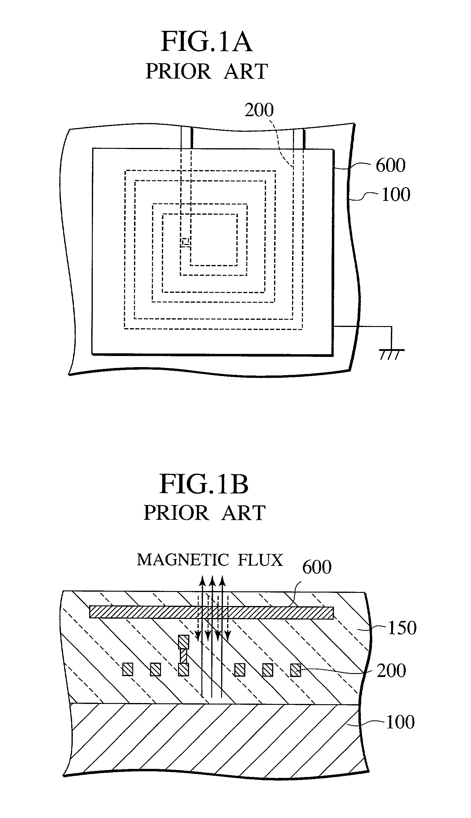
Semiconductor device with a spiral inductor
a spiral inductor and electromagnetic shielding technology, applied in the direction of solid-state devices, inductances, magnetic/electric field screening, etc., can solve the problem of difficult to obtain a sufficient electromagnetic shielding
- Summary
- Abstract
- Description
- Claims
- Application Information
AI Technical Summary
Benefits of technology
Problems solved by technology
Method used
Image

Examples
first embodiment
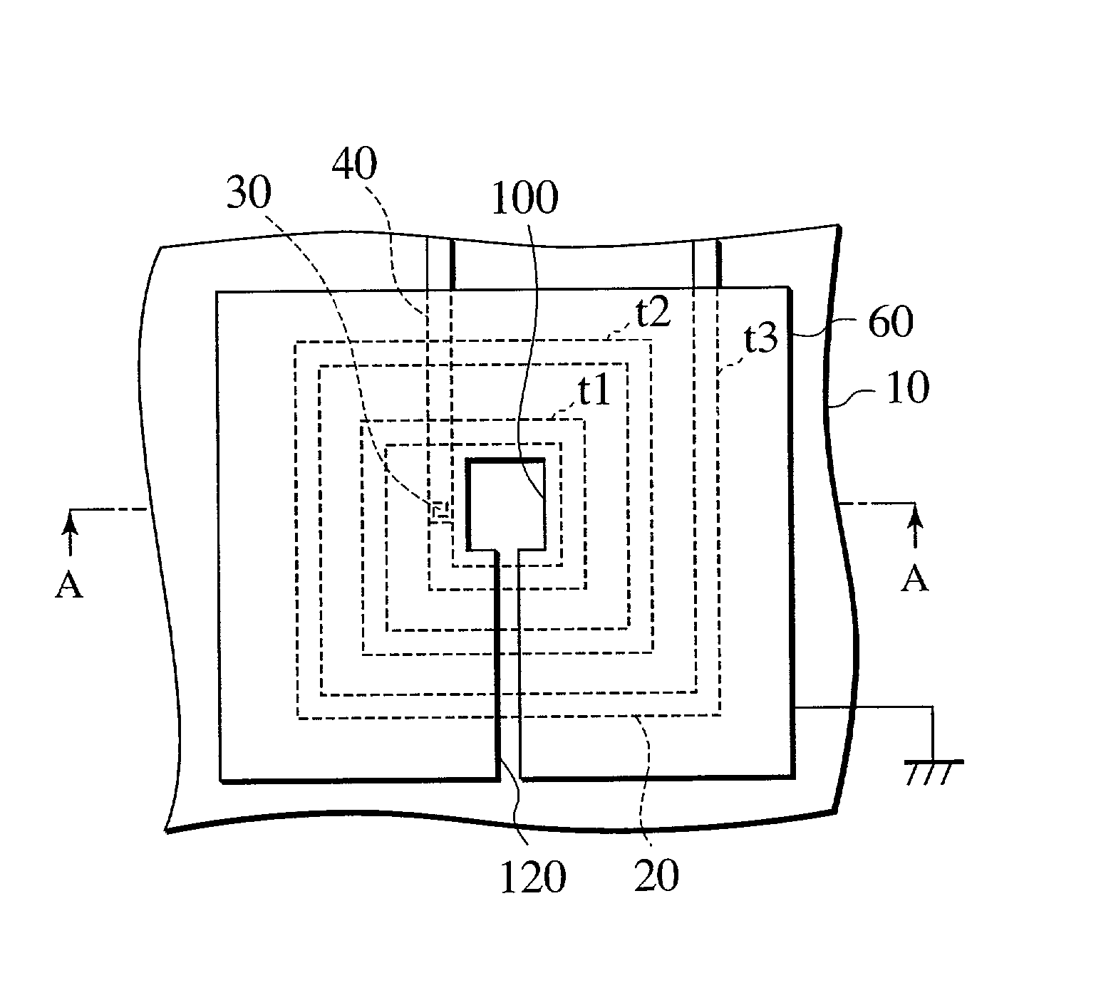
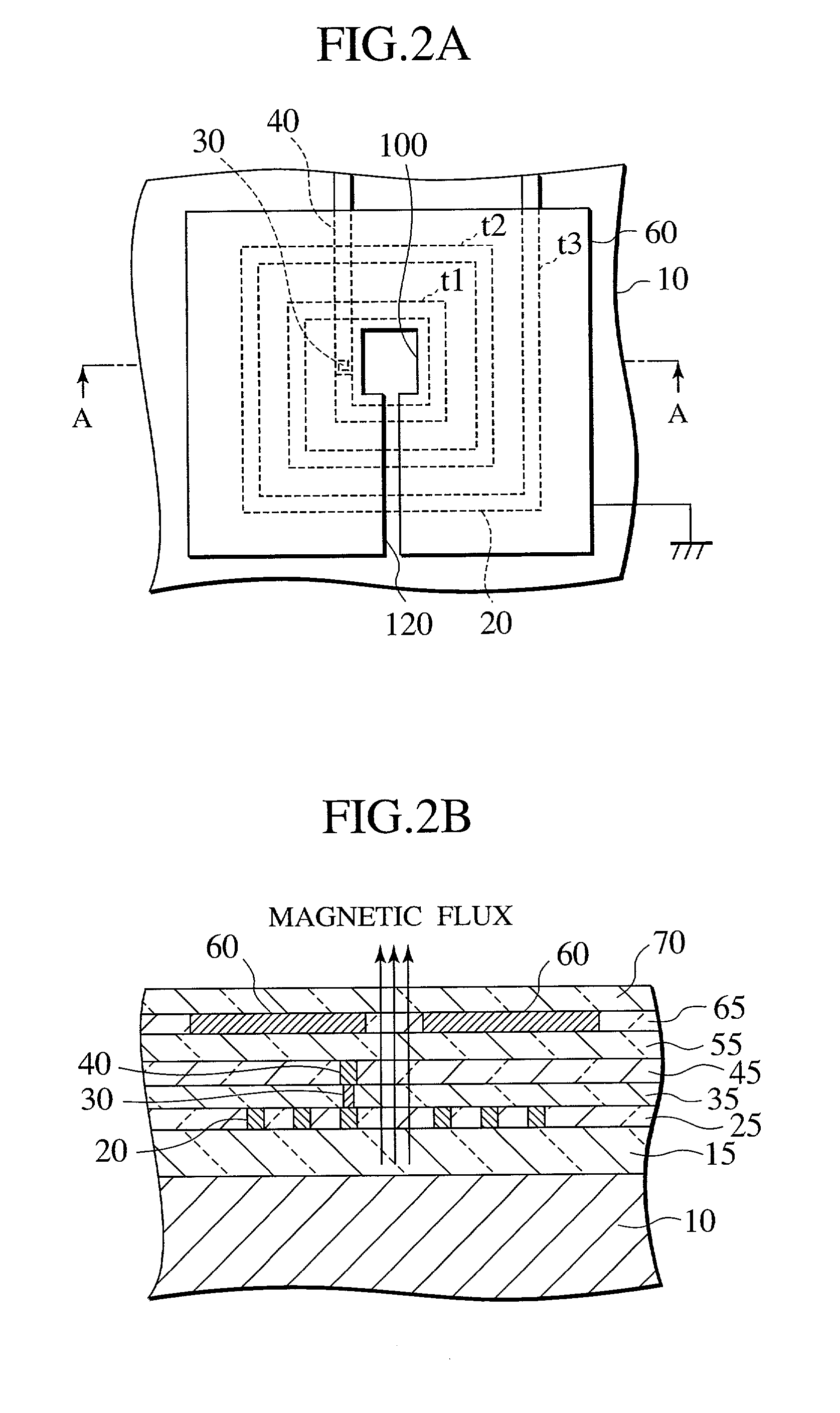
[0024] FIG. 2A is a plan view showing a first embodiment of a semiconductor device of the present invention, and FIG. 2B is a sectional view taken along a break line A-A in FIG. 2A.
[0025] As shown in FIG. 2A, the semiconductor device according to the first embodiment includes a spiral inductor 20 having a spiral pattern formed on the same plane and an electromagnetic wave shield 60. For example, a spiral pattern is shown here, which has first, second and third turns t1, t2 and t3 from the inside. The electromagnetic wave shield 60 has an opening 100 in a region above an approximately central region of the spiral pattern of the spiral inductor 20 and has a slit 120 extending from this opening 100 to a peripheral portion of the electromagnetic wave shield 60.
[0026] Hereinafter, description will be made more concretely for a constitution of each portion.
[0027] A formation position of the spiral inductor is not particularly limited, and the spiral inductor may be formed of any of wiring...
second embodiment
[0044] FIG. 3A is a plan view showing a second embodiment of the semiconductor device of the present invention, and FIG. 3B is a sectional view taken along a break line B-B in FIG. 3A.
[0045] Similarly to the first embodiment, also in the second embodiment, an electromagnetic wave shield has an opening in a region facing to an approximately central region of a spiral pattern of a spiral inductor, and has a slit reaching a peripheral portion of the electromagnetic wave shield from this opening. However, the second embodiment is different from the first embodiment in that the electromagnetic wave shield is formed below the spiral inductor.
[0046] As shown in FIG. 3A and FIG. 3B, similarly to the first embodiment, a first wiring layer on the first interlayer insulating film 15 formed on the semiconductor substrate 10 is patterned, and the spiral inductor 20 having a spiral pattern in a swirl shape is formed. As a size and a shape of the spiral inductor 20, the ones under approximately th...
third embodiment
[0052] FIG. 4A is a plan view showing a third embodiment of the semiconductor device of the present invention, and FIG. 4B is a sectional view taken along a break line C-C in FIG. 4A.
[0053] Similarly to the first and second embodiments, also in the third embodiment, an electromagnetic wave shield has an opening in a central region of a spiral pattern of a spiral inductor, that is, in a region corresponding to a region above the region in the inside of the first turn t1 in the innermost side, and has a slit reaching a peripheral portion of the electromagnetic wave shield from this opening. However, the third embodiment is different from the first and second embodiments in that the electromagnetic wave shields are formed above and below the spiral inductor.
[0054] As shown in FIG. 4A and FIG. 4B, similarly to the first and second embodiments, in a first wiring layer on the first interlayer insulating film 15 formed on the semiconductor substrate 10, the spiral inductor 20 of a spiral p...
PUM
| Property | Measurement | Unit |
|---|---|---|
| width | aaaaa | aaaaa |
| thickness | aaaaa | aaaaa |
| width | aaaaa | aaaaa |
Abstract
Description
Claims
Application Information