Pin attachment by a surface mounting method for fabricating organic pin grid array packages

a surface mounting and organic technology, applied in the direction of sustainable manufacturing/processing, final product manufacturing, soldering apparatus, etc., can solve the problems of affecting the miniaturization of electronic products, the surface mounting method is undoubtedly doubt a lower cost manufacturing method, and the change is often difficult to achieve. , to achieve the effect of improving the strength and reliability of the solder join

Inactive Publication Date: 2002-12-05
PHOENIX PRECISION TECH CORP
View PDF0 Cites 10 Cited by
  • Summary
  • Abstract
  • Description
  • Claims
  • Application Information

AI Technical Summary

Benefits of technology

0013] It is therefore an objective of the present invention to provide a surface mounting method for attaching the pins onto an organic PGA substrate, which is able to result in improved strength and reliability of the solder joint in a PGA package used to electrically interconnect with a socket or an adaptor.

Problems solved by technology

However, such changes are often difficult to achieve, because currently a variety of the packaged electrical components are generally soldered to a printed circuit board by means of either the surface mounting technique or through-hole mounting technique.
The major disadvantage with the through-hole technique is that the through hole should be large (e.g. at least larger than 15 mil in diameter) for through-soldering being feasible, which however adversely impacts miniaturization of electronic products.
However, the surface mounting method is undoubtedly doubt a lower cost manufacturing method compared to the through-hole technique, since the processing step to form the holes for receiving the pins in the wiring substrate could be skipped.

Method used


Image

  • Pin attachment by a surface mounting method for fabricating organic pin grid array packages
  • Pin attachment by a surface mounting method for fabricating organic pin grid array packages
  • Pin attachment by a surface mounting method for fabricating organic pin grid array packages

Examples


Embodiment Construction

[0027] For a better understanding on the advantages and capabilities of the present invention, reference is made to the following disclosure, appended claims in connection with the accompanying drawings.

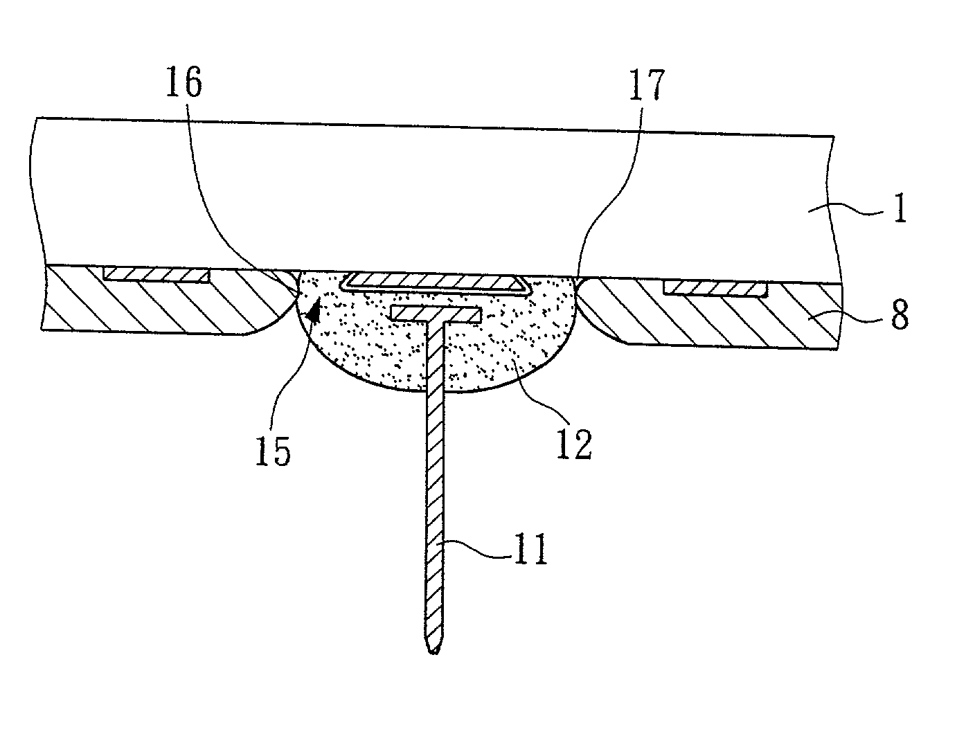
[0028] The invention provides a surface mounting method for attaching the pins onto an organic PGA substrate, which is able to result in improved strength and reliability of the solder joint in a PGA package used to electrically interconnect with a socket or an adaptor. The method is detailed as follows. Like numbers refer to like elements throughout. However, the figures are simply illustrative of the process, and are not drawn to scale, i.e. they do not reflect the actual dimensions or features of the various layers in the chip package structure.

[0029] Now referring to FIG. 4A, in accordance with a preferred embodiment of the present invention, there is initially provided an organic wiring substrate 1, which has the wiring circuit layers 2 separated by the organic insulating layers...


PUM

PropertyMeasurementUnit
diameteraaaaaaaaaa
diameteraaaaaaaaaa
thicknessaaaaaaaaaa

Abstract

A pin attachment method for mounting the pins on a wiring substrate for fabricating a pin grid array package is disclosed. There is provided an organic wiring board including a surface bearing electrical circuitry which includes at least one contact pad for receiving a pin. A solder mask layer which is placed on the board surface and patterned to expose the pad. The solder mask layer which does not cover any portion of the pad and forms a well by the perimeter of the solder mask layer around the pad. Subsequently, a pin and a solder material which are placed over said pad in the well. The pin which is soldered to the pad by a temperature sufficient to melt the solder material.

Description

[0001] 1. Field of Invention[0002] This invention relates generally to organic pin grid array packages. More particularly, the present invention relates to a method of surface mounting the pins for fabricating an organic pin grid array package.[0003] 2. Background of the Invention[0004] There are many instances, in which under functional or economic considerations it is desirable to be able to alter the set of electrical components on a circuit board but simultaneously be able to avoid the expense of a board redesign or replacement of an otherwise good circuit board. For example, a computer user may hope to upgrade a computer to include a more powerful and lower voltage-supply microprocessor to replace the old one. However, such changes are often difficult to achieve, because currently a variety of the packaged electrical components are generally soldered to a printed circuit board by means of either the surface mounting technique or through-hole mounting technique.[0005] It has bee...

Claims


Application Information

Patent Timeline
Patent Type & Authority Applications(United States)
IPC IPC(8): H01L21/48H01L23/498H05K3/34
CPCH01L21/4853H01L24/49H01L2224/16225H01L2224/32225H01L2224/48091H01L2224/49109H01L2924/01012H01L2924/01046H01L2924/01078H01L2924/01079H01L2924/15312H01L2924/1532H05K3/3421H05K3/3426H05K3/3452H05K2201/09036H05K2201/09472H05K2201/0989H05K2201/10318H05K2201/10787H01L23/49811H01L24/48H01L2924/00014H01L2224/45099H01L2924/14H01L2924/181Y02P70/50H01L2224/45015H01L2924/207H01L2924/00H01L2924/00012
Inventor TUNG, I-CHUNGHSU, SHIH-PING
Owner PHOENIX PRECISION TECH CORP
Why Eureka
Try Eureka