Automated overlay metrology system

a metrology system and overlay technology, applied in semiconductor/solid-state device testing/measurement, semiconductor/solid-state device details, instruments, etc., can solve the problems of reducing the minimum feature size, reducing the manufacturing yield, and expensive sem or afm tools

Inactive Publication Date: 2002-12-19
NIKON CORP
View PDF0 Cites 93 Cited by
  • Summary
  • Abstract
  • Description
  • Claims
  • Application Information

AI Technical Summary

Problems solved by technology

However, such measurement techniques require complex and expensive SEM or AFM tools which are inherently of low throughput and the measurement is necessarily destructive, decreasing manufacturing yield.
Perhaps more importantly, decreases in minimum feature size and increases in integration density have required increasingly complex, expensive and difficult to use measurement tools while measurements produced are of reduced repeatability, reproducibility, tool induced shift (which are the principal components of the metrology error budget) and quantitative certainty (e.g. confidence factor) as limits of both lithographic and microscopic resolutions are app

Method used


Image

  • Automated overlay metrology system
  • Automated overlay metrology system
  • Automated overlay metrology system

Examples


Embodiment Construction

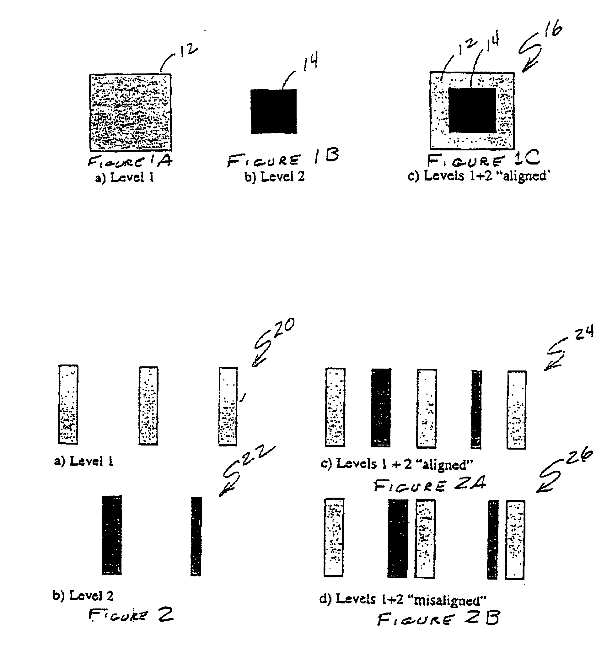
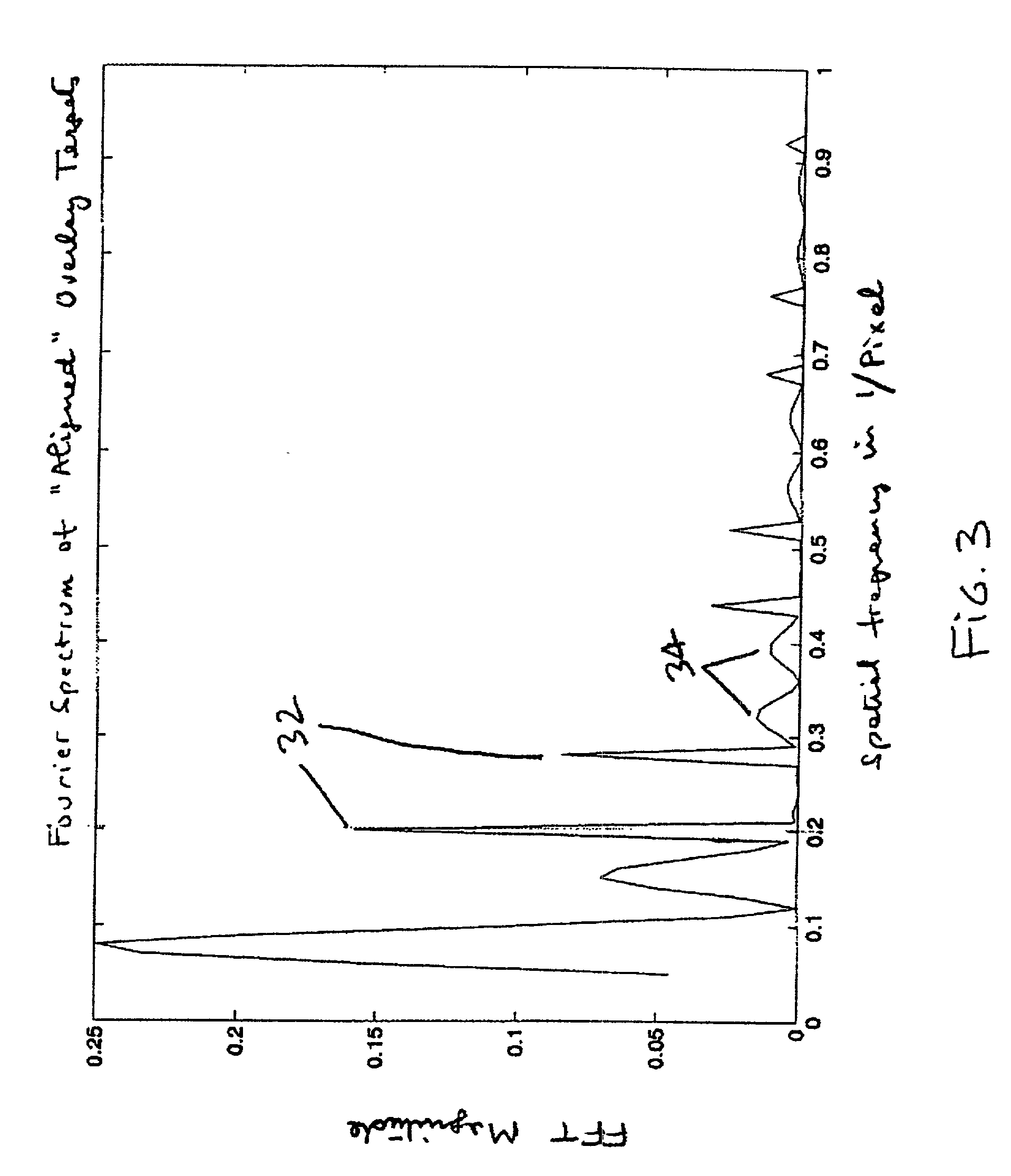
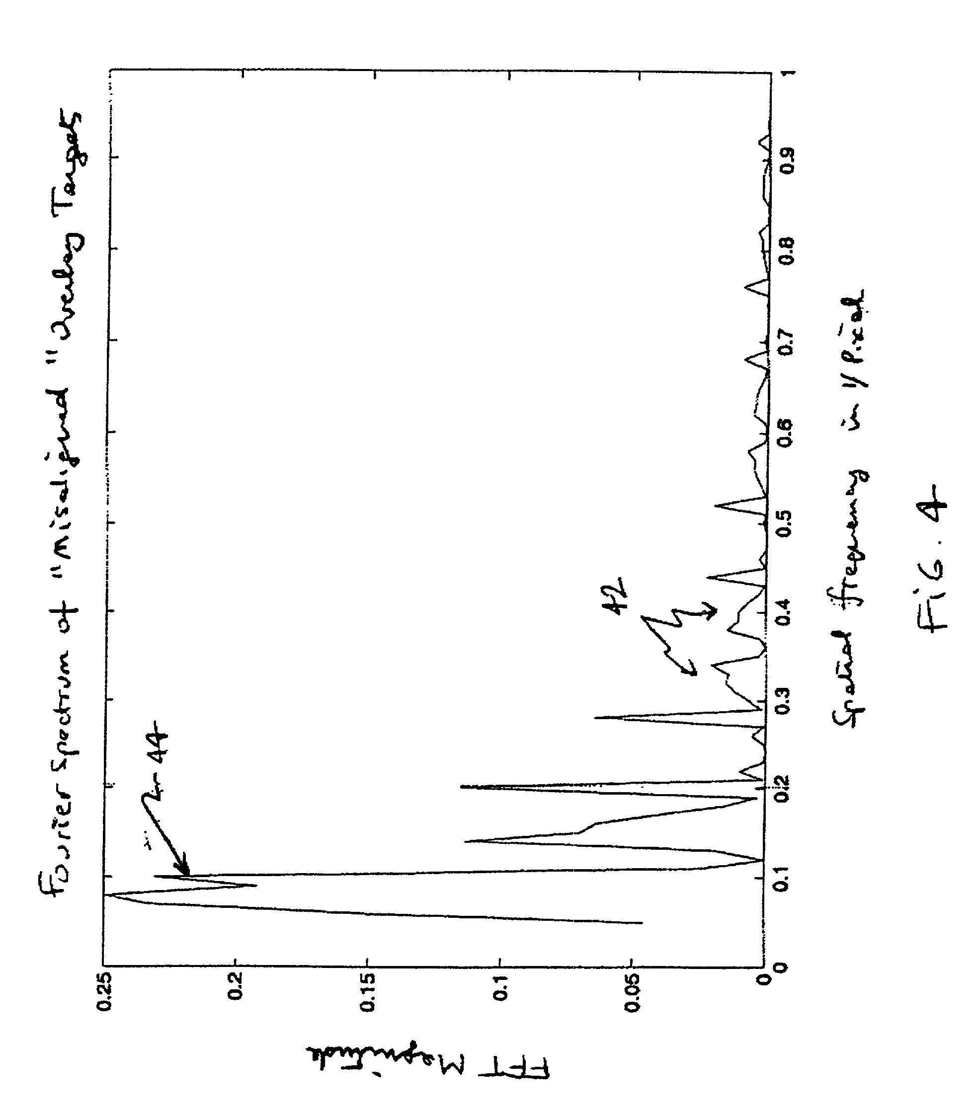
[0028] Referring now to the drawings, and more particularly to FIGS. 1A, 1B and 1C, there is shown a typical box-in-box metrology feature exemplary of features for such purposes known and used in the art. The box-in-box feature 16 shown in FIG. 1C is a composite feature formed by two overlaid lithographic exposures corresponding respectively to features 12 and 24 of FIGS. 1A and 1B, respectively, which are generally sequentially performed and each preceded by deposition of a layer of resist and followed by development of resist layer and possibly including etching or material deposition processes between the lithographic exposures. One feature will be larger than the other and the smaller feature should be of dimensions which, ideally, closely approach the minimum feature size of interest.

[0029] At the present state of the art, however, the smaller and larger features are generally produced with a transverse dimension of the order of a few microns. Such dimensions are about an order...


PUM


Abstract

Non-imaging measurement is made of misalignment of lithographic exposures by illuminating periodic features of a mark formed by two lithographic exposures with broadband light and detecting an interference pattern at different wavelengths using a specular spectroscopic scatterometer including a wavelength dispersive detector. Misalignment can be discriminated by inspection of a spectral response curve and by comparison with stored spectral response curves that may be empirical data or derived by simulation. Determination of best fit to a stored spectral curve, preferably using an optimization technique can be used to quantify the detected misalignment. Such a measurement may be made on-line or in-line in a short time while avoiding tool induced shift, contact with the mark or use of a tool requiring high vacuum.

Description

[0001] 1. Field of the Invention[0002] The present invention generally relates to multiple sequential lithography processes and, more particularly, to metrology techniques for measurement and characterization of overlay and alignment accuracy for sequential lithographic exposures and in-line and on-line lithographic exposure, scanner or stepper tools.[0003] 2. Description of the Prior Art[0004] Lithography processes are currently used in many research and manufacturing environments. Among these environments, one of the more economically important is that of semiconductor integrated circuit manufacture. In this field, increased functionality, performance and potential economy of manufacture has driven the development of numerous successive generations of devices having minimum feature size regimes of increasingly small dimensions and correspondingly increased device density. Currently, feature size regimes of one-quarter micron are available in commercial devices with significant fur...

Claims


Application Information

Patent Timeline
IPC IPC(8): G03F7/20G03F9/00H01L21/027G01B11/24H01L23/544
CPCG03F7/70633H01L22/34H01L2924/0002H01L2924/00
Inventor FAY, BERNARDAIYER, ARUN A.
Owner NIKON CORP
Why Eureka
Try Eureka