Semiconductor device and method for manufacturing the same

a technology of semiconductor devices and semiconductors, applied in semiconductor devices, capacitors, electrical devices, etc., can solve problems such as complex processes

Inactive Publication Date: 2002-12-26
SAMSUNG ELECTRONICS CO LTD
View PDF0 Cites 96 Cited by
  • Summary
  • Abstract
  • Description
  • Claims
  • Application Information

AI Technical Summary

Benefits of technology

[0014] A stabilizing layer, such as a silicon oxide layer, a silicon nitride layer, or a composite layer of the silicon oxide layer and the silicon nitride layer, for facilitating the formation of the dielectric layer by hydrophilizing the surface of the first electrode can also be formed on the first electrode. The dielectric layer can be formed by an atomic layer deposition method.
[0015] According to the present invention, the silicon-family material is used as the lower electrode. The dielectric layer is formed by an atomic layer deposition method, and the upper electrode is formed of a material layer having a work function larger than that of the lower electrode. Accordingly, it is possible to improve the insulating characteristic of the dielectric layer and to increase the capacitance value in the capacitor structure.

Problems solved by technology

However, when the high dielectric layer, such as the tantalum oxide layer (Ta.sub.2O.sub.5) or the BST (BaSrTiO.sub.3) layer, is used as the dielectric layer, processes become complicated since subsequent processes are needed in order to obtain a stable capacitor.

Method used


Image

  • Semiconductor device and method for manufacturing the same
  • Semiconductor device and method for manufacturing the same
  • Semiconductor device and method for manufacturing the same

Examples


Embodiment Construction

[0028] Illustrative embodiments of the present invention will now be described with reference to the accompanying FIGURES.

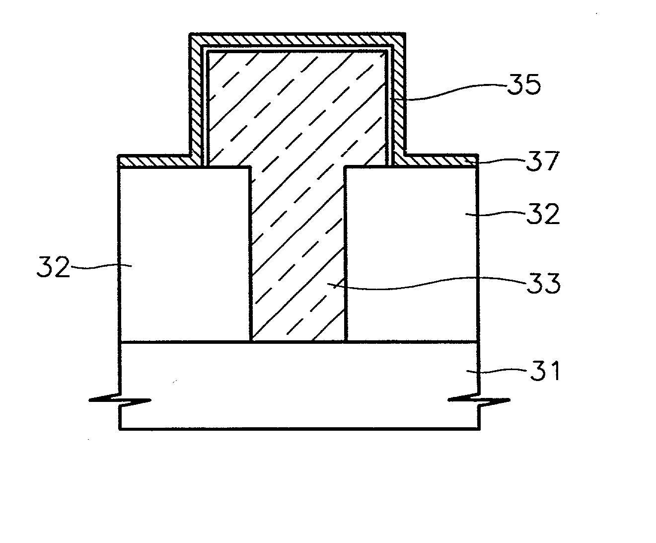
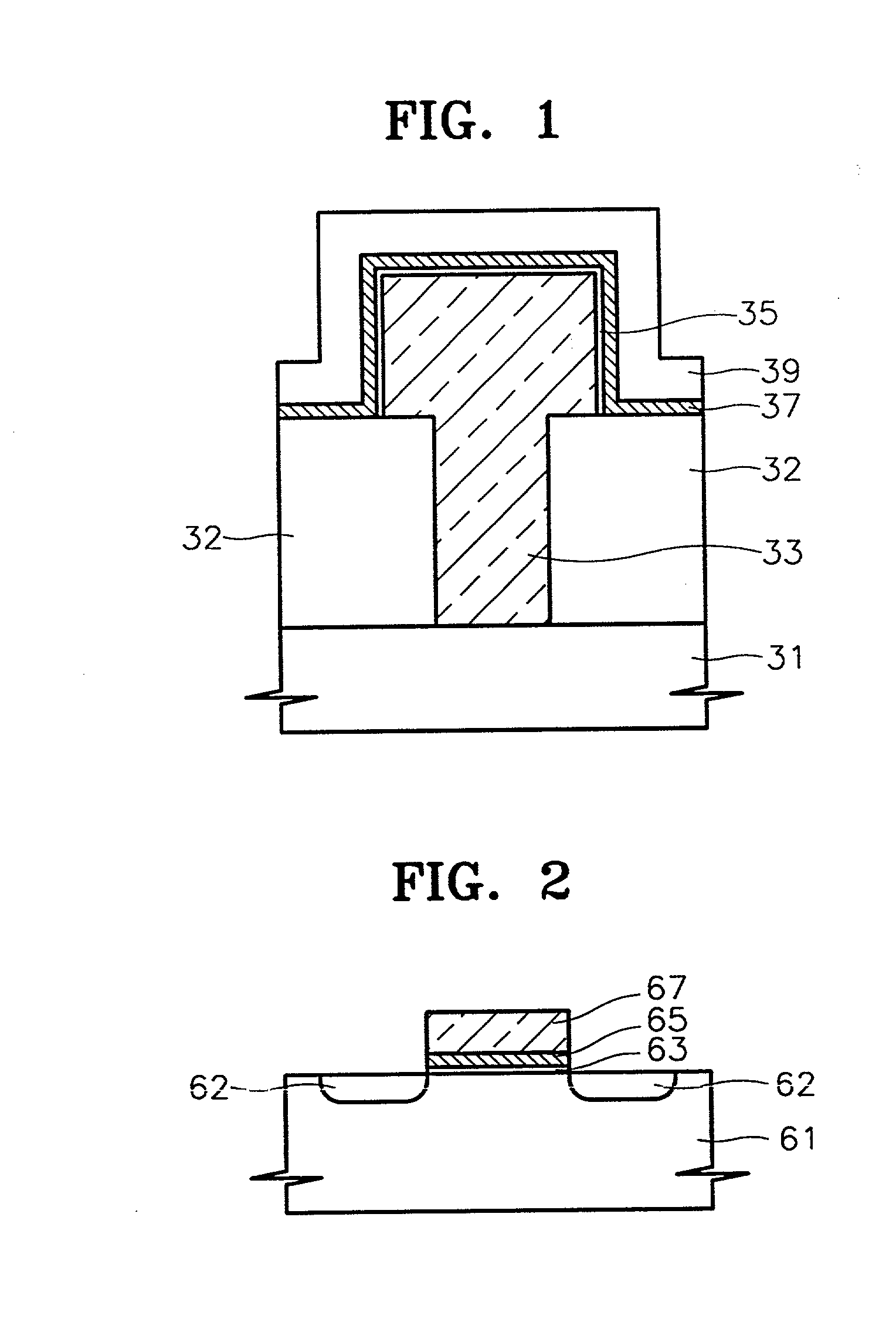
[0029] FIG. 1 is a cross-sectional view showing a semiconductor device according to a first embodiment of the present invention. More specifically, the semiconductor device according to the present invention has a capacitor structure. Namely, the semiconductor device of the present invention includes lower electrode 33 of a capacitor, dielectric layer 37, and upper electrode 39 of the capacitor used as a second electrode. All elements, lower electrode 33, dielectric layer 37 and upper electrode 39 are formed on semiconductor substrate 31, which is, i.e., a silicon substrate used as a first electrode. In FIG. 1, reference numeral 32 denotes an inter level dielectric layer.

[0030] Lower electrode 33 is formed of a layer made of a silicon-family material from which a three-dimensional structure is easily formed, e.g., a polysilicon layer doped with impurities such as...


PUM


Abstract

A semiconductor device includes a first electrode formed of a silicon-family material, a dielectric layer formed by sequentially supplying reactants on the first electrode, and a second electrode having a work function larger than that of the first electrode, with the second electrode being formed on the dielectric layer. The first electrode and the second electrode can be a lower electrode and an upper electrode, respectively, in a capacitor structure. Also, the first electrode and the second electrode can be a silicon substrate and a gate electrode, respectively, in a transistor structure. A stabilizing layer, which is, for example, a silicon oxide layer, a silicon nitride layer, or a composite layer of the silicon oxide layer and the silicon nitride layer, for facilitating the formation of the dielectric layer by hydrophilizing the surface of the first electrode, may be formed on the first electrode. The dielectric layer can be formed by an atomic layer deposition method. Accordingly, in the semiconductor device, it is possible to improve the insulating characteristic of the dielectric layer and to increase a capacitance value in the capacitor structure.

Description

[0001] This application is based upon and claims priority from Korean Patent Application No. 99-33520 filed Aug. 14, 1999, the contents of which are incorporated herein by reference.[0002] 1. Field of the Invention[0003] The present invention relates to a semiconductor device and a method for manufacturing the same. More particularly, the present invention relates to a semiconductor device in which it is possible to improve the insulating characteristics of a high dielectric layer (a dielectric layer with a large dielectric constant) when a semiconductor material is used as a lower electrode. The invention also relates to a method for manufacturing the same.[0004] 2. Description of the Related Art[0005] Normally, semiconductor devices have a structure in which a dielectric layer is formed between a lower electrode and an upper electrode. For example, a transistor structure in which a dielectric layer (a gate insulating layer) and a gate electrode are sequentially formed on a silicon...

Claims


Application Information

Patent Timeline
Patent Type & Authority Applications(United States)
IPC IPC(8): H01L29/43H01L21/02H01L21/28H01L21/316H01L21/318H01L21/822H01L21/8242H01L21/8246H01L27/04H01L27/10H01L27/105H01L27/108H01L29/423H01L29/49H01L29/51
CPCH01L21/28194H01L28/55H01L29/518H01L29/513H01L29/517H01L28/60H01L27/10
Inventor KIM, YEONG-KWANPARK, HEUNG-SOOPARK, YOUNG-WOOKLEE, SANG-INCHANG, YOON-HEELEE, JONG-HOCHOI, SUNG-JELEE, SEUNG-HWANLIM, JAE-SOONLEE, JOO-WON
Owner SAMSUNG ELECTRONICS CO LTD
Why Eureka
Try Eureka