Integrated EMC shield for integrated circuits and multiple chip modules

a technology of integrated circuits and chip modules, applied in the field of semiconductor packages, can solve the problems of adding work steps and requiring additional space on the pcb

Inactive Publication Date: 2003-01-02
NOKIA CORP
View PDF0 Cites 47 Cited by
  • Summary
  • Abstract
  • Description
  • Claims
  • Application Information

AI Technical Summary

Problems solved by technology

This requires additional space on the PCB and adds a workstep during assembly of the PCB.

Method used


Image

  • Integrated EMC shield for integrated circuits and multiple chip modules
  • Integrated EMC shield for integrated circuits and multiple chip modules
  • Integrated EMC shield for integrated circuits and multiple chip modules

Examples


Embodiment Construction

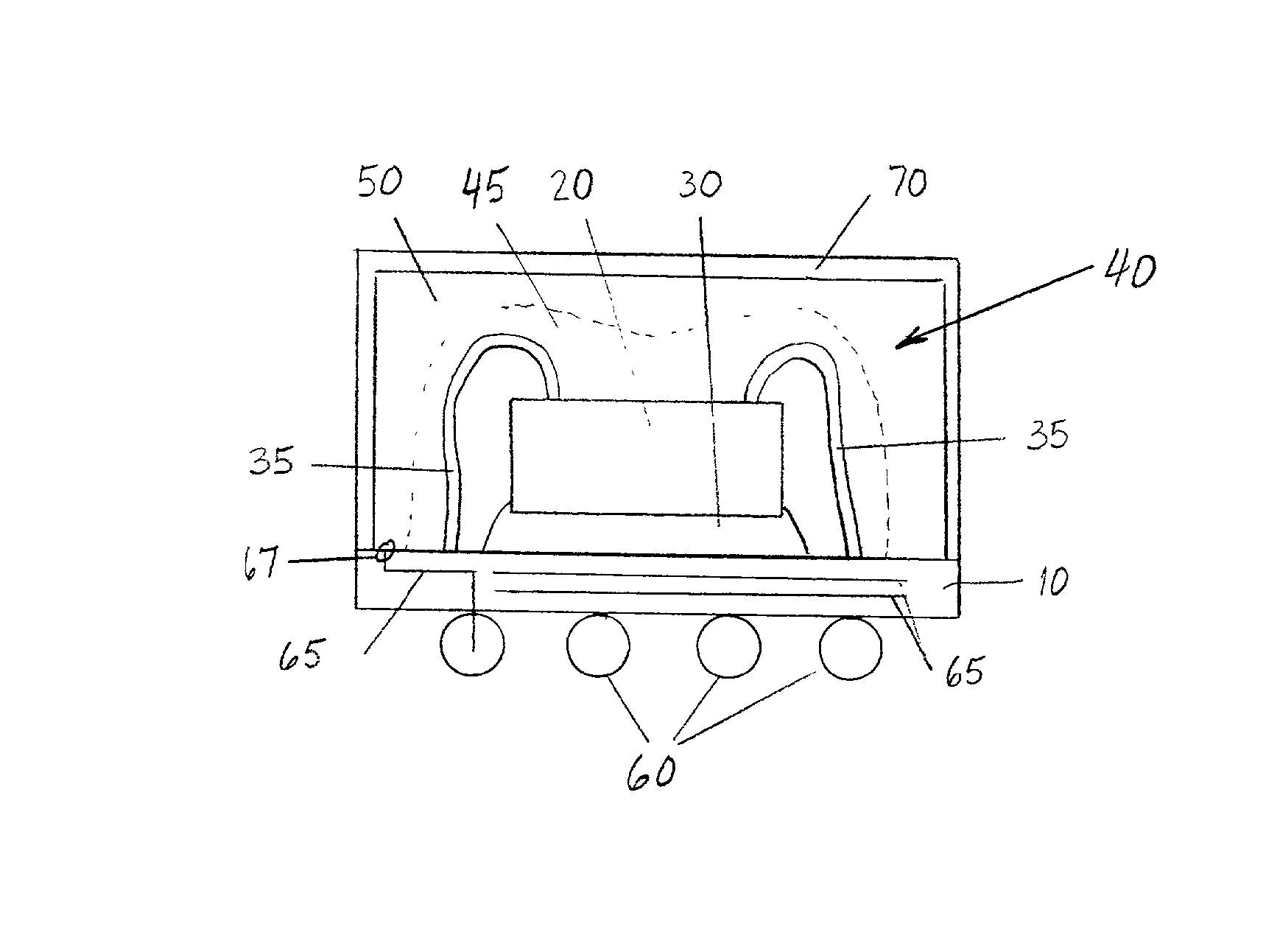
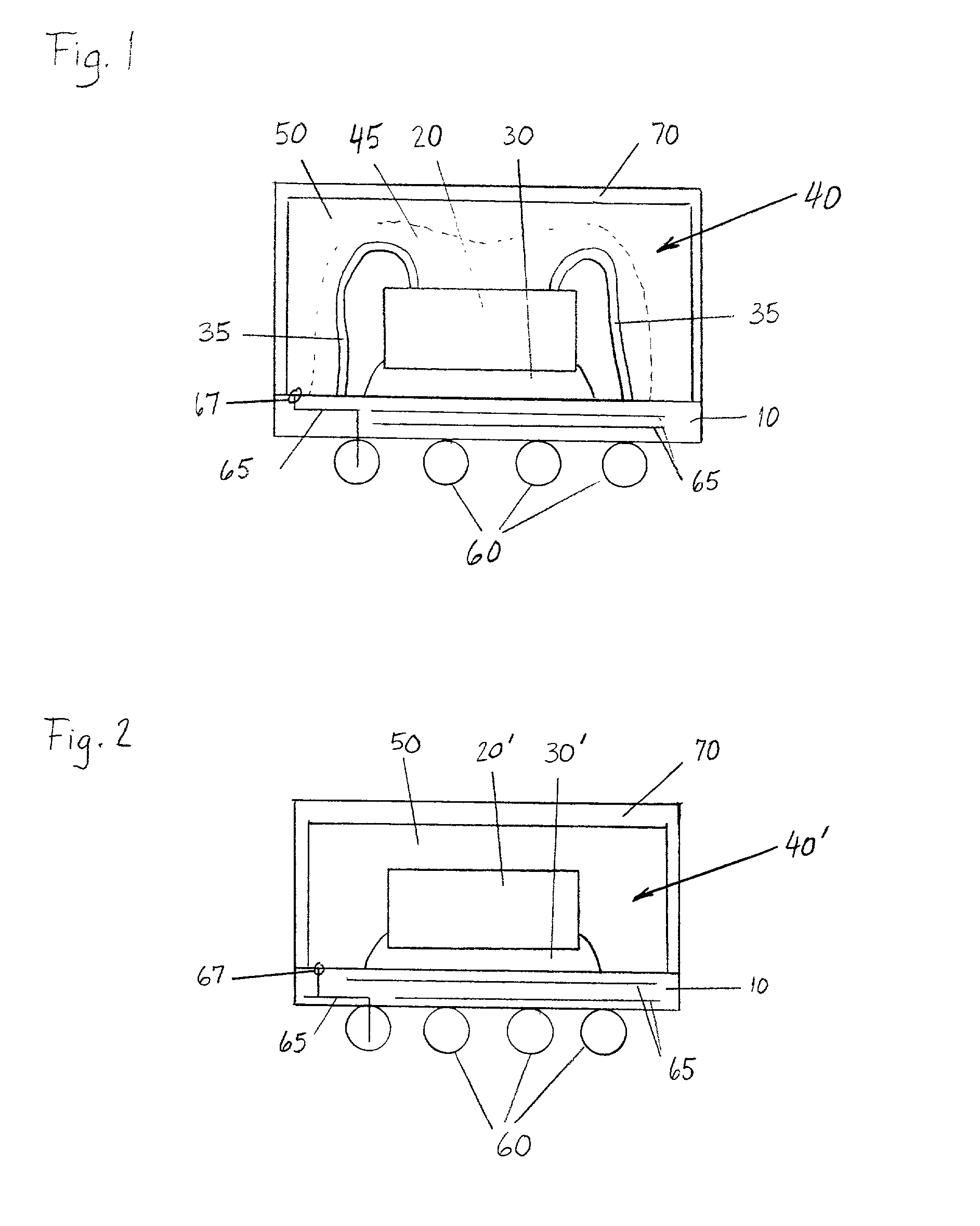
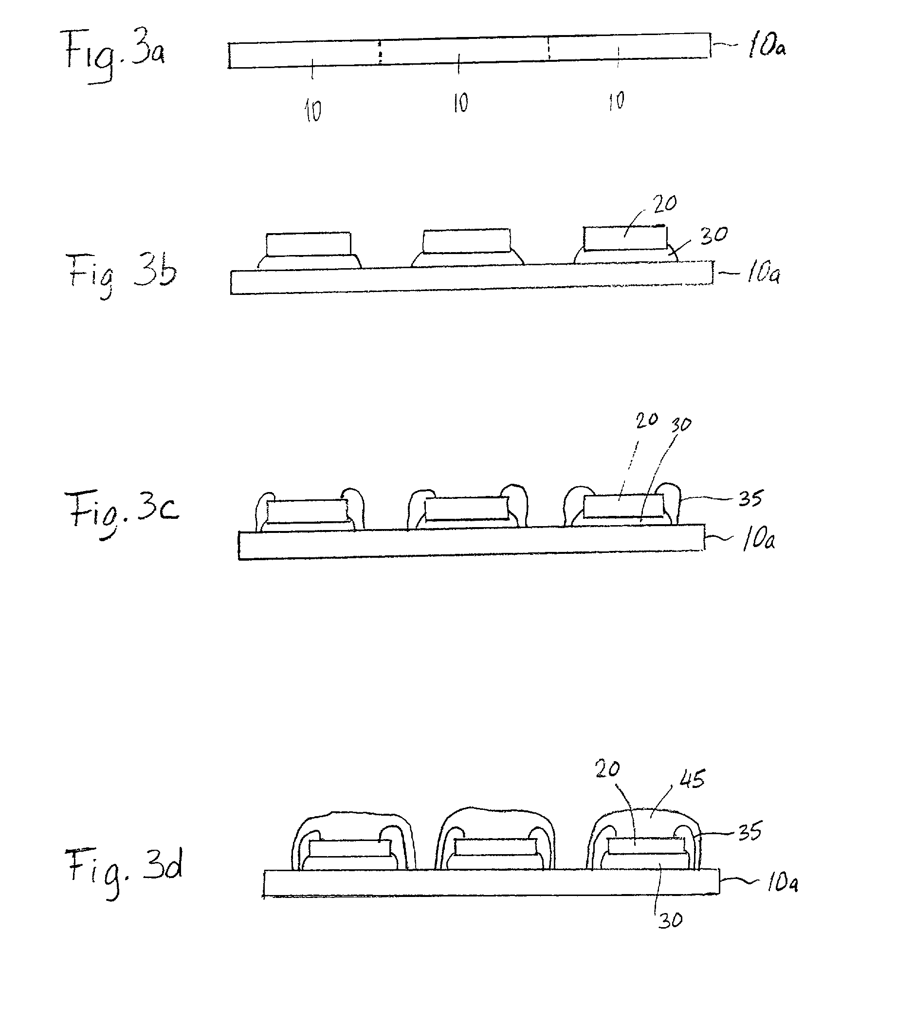
[0016] FIG. 1 discloses a semiconductor package according to a first embodiment of the present invention. The semiconductor package includes a printed circuit board (PCB) 10 on which a die 20, i.e., a semiconductor chip, is arranged. The PCB 10 includes routing wires 65 which are arranged under a mask (not shown). The die 20 comprises a wire bonded die in that the die 20 is electrically connected to routing wires 65 of the PCB 10 via wires 35. The die 20 is physically attached or held onto the PCB 10 by a connection 30 which may, for example, comprise glue or solder.

[0017] A transfer molding 40 encapsulates the die 20 on the PCB 10. The transfer molding 40 includes a non-conductive material 45 which encapsulates the wires 35 and the die 20 on the PCB 10, and a conductive material 50 that covers the non-conductive material 45 and provides an electromagnetic compatibility (EMC) shield for the die 20. The non-conductive material 45 may comprise a non-conductive material such, for examp...


PUM

PropertyMeasurementUnit
conductiveaaaaaaaaaa
electrically conductingaaaaaaaaaa
electrically conductiveaaaaaaaaaa

Abstract

A semiconductor package has a die connected to a substrate with a transfer molding applied over the die. The transfer molding includes an electrically conductive material for forming an electromagnetic compatibility shield as an integral part thereof.

Description

[0001] 1. Field of the Invention[0002] The present invention relates to a semiconductor package including a die arranged on a substrate and a transfer molding having an integrated electromagnetic compatibility (EMC) shield for integrated circuits and for multiple chip modules, and to a method for manufacturing the semiconductor package with the integrated EMC shield.[0003] 2. Description of the Related Art[0004] Known semiconductor packages which include a die or multiple dies, such as an integrated circuit (IC) or a multiple chip module (MCM), are encased in a transfer molding made of an insulating or dielectric material as disclosed in U.S. Pat. No. 6,087,202. The semiconductor package is a unit that is installed on a printed circuit board (PCB) with other components as part of a larger device. If a particular application of the known semiconductor package requires an EMC shield, a separate EMC shield is arranged around the semiconductor package on the PCB. This requires additiona...

Claims


Application Information

Patent Timeline
Patent Type & Authority Applications(United States)
IPC IPC(8): H01L23/31H01L23/552
CPCH01L23/3128Y10T29/49146H01L24/97H01L2221/68331H01L2224/48227H01L2224/97H01L2924/14H01L2924/15311H01L2924/16152H01L2924/3025H01L23/552Y10T29/4913H01L2224/73265H01L2224/32225H01L2924/01033H01L2924/01005H01L24/48H01L2224/85H01L2924/00012H01L2924/00H01L2924/181H01L24/73H01L2224/05599H01L2224/45099H01L2224/85399H01L2924/00014H01L2924/15184H01L2224/45015H01L2924/207
Inventor NURMINEN, JANNE
Owner NOKIA CORP
Why Eureka
Try Eureka