Power semiconductor apparatus

a technology of power semiconductor and sealing type, which is applied in the direction of solid-state devices, electrical apparatus construction details, basic electric elements, etc., can solve the problems of low productivity, increase in the size of the power semiconductor apparatus, and low current carrying capacity of the conventional power semiconductor apparatus. achieve the effect of improving productivity, cost reduction and high reliability

Inactive Publication Date: 2010-06-03
MITSUBISHI ELECTRIC CORP
View PDF5 Cites 39 Cited by
  • Summary
  • Abstract
  • Description
  • Claims
  • Application Information

AI Technical Summary

Benefits of technology

[0010]This invention has been accomplished to solve the problems such as described above, and it is an object of the invention to provide a power semiconductor apparatus formed by sealing with a transfer mold resin that achieves an improvement in the productivity and a cost reduction and that can be used with high reliability even under high current and high voltage.

Problems solved by technology

Thus, the conventional power semiconductor apparatus requires many manufacturing steps and a long manufacturing time, resulting in low productivity.
Moreover, this conventional power semiconductor apparatus has a low current carrying capacity per the area of the base of the module.
Therefore, a problem arises that the size of the power semiconductor apparatus increases.
However, with the method using the lead frame 25, the external terminals are inevitably exposed in one row from a side face of the power semiconductor apparatus because of the constraints of the manufacturing process.
However, with such a conventional method that the external terminals are exposed in one row, there is no other method than increasing the size of the power semiconductor apparatus itself in order to ensure a high withstand voltage, so the apparatus inevitably becomes larger.
Therefore, if a defect occurs in any of the components in the apparatus, the entire apparatus needs to be replaced.
This leads to the problems of a degradation of the product yield and high costs in the manufacture.

Method used


Image

  • Power semiconductor apparatus
  • Power semiconductor apparatus
  • Power semiconductor apparatus

Examples


embodiment 1

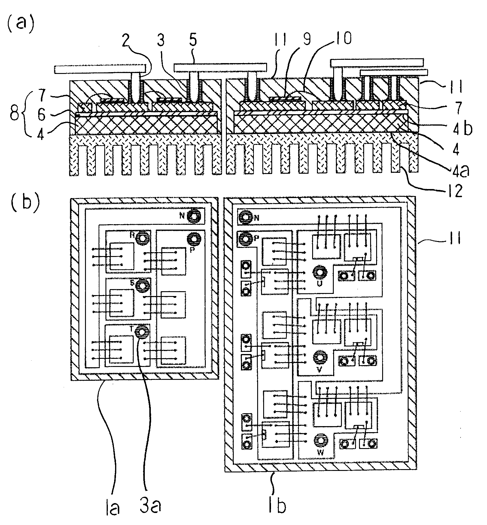
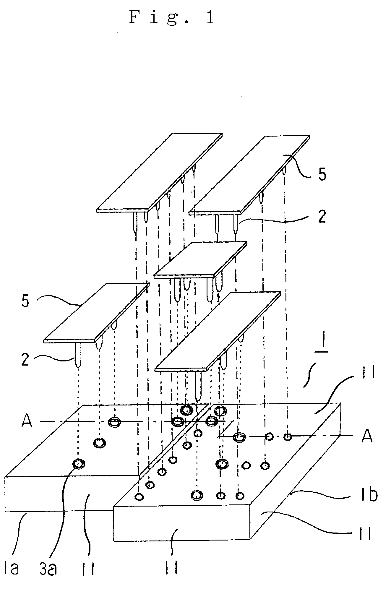
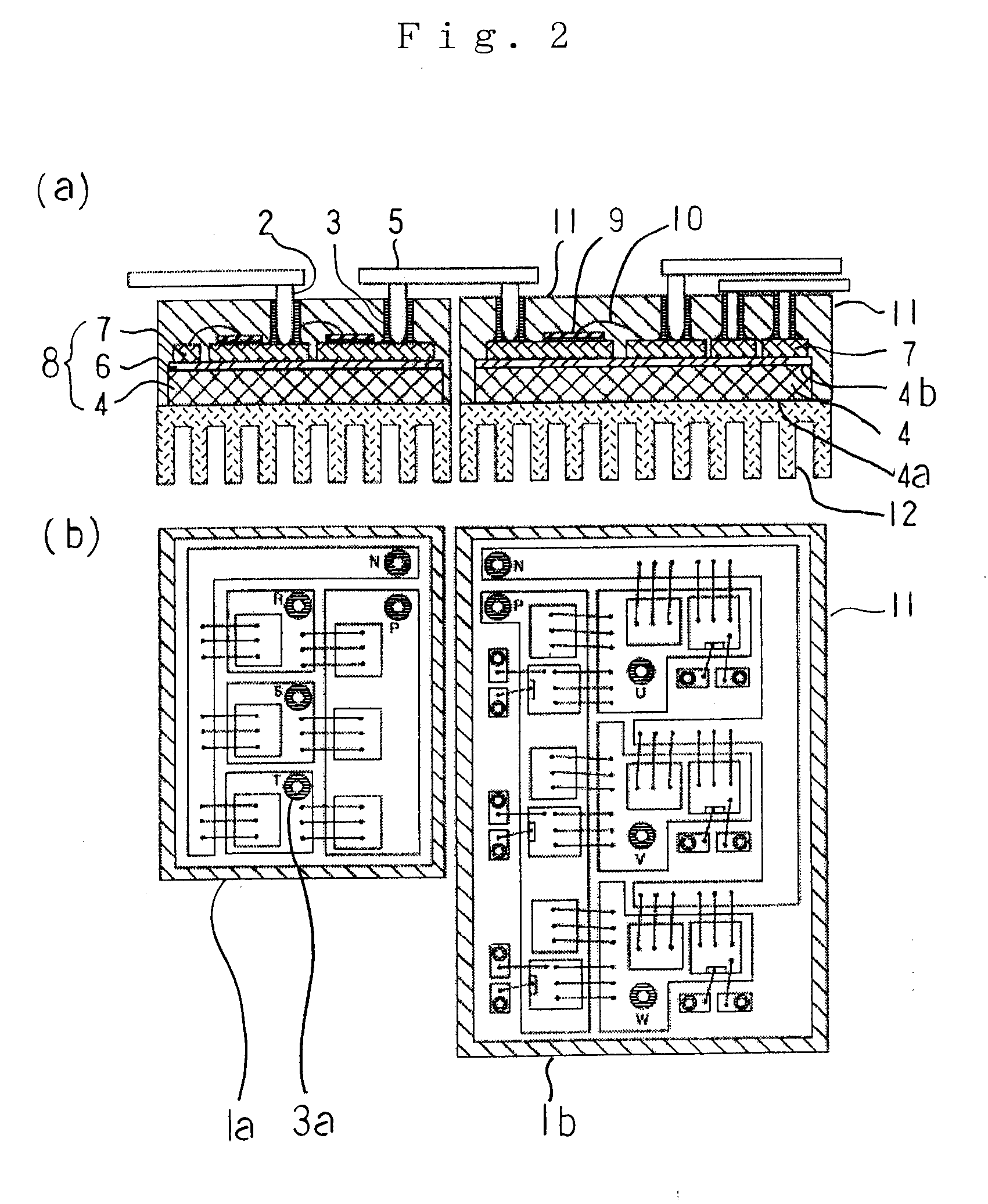
[0021]FIG. 1 is an exploded perspective view showing a power semiconductor apparatus before assembled, according to Embodiment 1 of the invention. FIG. 2A is a cross-sectional view taken along line A-A of FIG. 1, showing the apparatus after assembled, and FIG. 2B is a cross-sectional view showing the apparatus in which conductive connecting members are removed therefrom and a transfer mold resin on a metal plate 4 is also removed. As shown in FIG. 1, a power semiconductor apparatus 1 of Embodiment 1 includes a plurality of power semiconductor units 1a and 1b combined together. Each of the power semiconductor units 1a and 1b is transfer-molded so as to expose insertion holes 3a of conductive tubular sockets 3, into which external terminals 2 can be inserted and connected, in one surface thereof and to expose a heat dissipation metal surface 4a for dissipating the heat of the metal plate 4 in the other surface. The power semiconductor apparatus 1 is provided with conductive connecting...

embodiment 2

[0037]FIG. 3 is an exploded perspective view showing a power semiconductor apparatus before assembled, according to Embodiment 2. FIG. 4A is a cross-sectional view taken along line B-B of FIG. 3, showing the apparatus after assembled, and FIG. 4B is a cross-sectional view showing the apparatus in which conductive connecting members are removed therefrom and a transfer mold resin on the metal plate 4 is also removed. In the drawings, the same reference symbols refer to the same or corresponding parts. Embodiment 2 is the same as Embodiment 1 except that the chip layout is different. As shown in FIG. 4, each of three power semiconductor units 1b is an inverter unit for one phase, each containing the anode side tubular sockets 3b and the cathode side tubular sockets 3c (that is, the upper and lower arms). Each of the power semiconductor units 1b, 1b, 1b (U, V, and W phases) that are the inverter units have the same configuration, and a three-phase inverter is constructed by connecting ...

embodiment 3

[0039]FIG. 5 is a cross-sectional view showing an apparatus of Embodiment 3 in which the conductive connecting members are removed therefrom and the transfer mold resin on the metal plate 4 is also removed. As shown in FIG. 5, a power semiconductor apparatus 1 of Embodiment 3 includes a converter unit and an inverter unit, which are power semiconductor units 1a and 1b. The power semiconductor apparatus 1 has the same configuration as that of Embodiment 1, except that anode side tubular sockets 3b and cathode side tubular sockets 3c (P·N sockets) of the power semiconductor units 1a and 1b are disposed so that the cathode side tubular sockets 3c surround the anode side tubular sockets 3b.

[0040]The cathode side tubular sockets 3c have a smaller diameter than the anode side tubular sockets 3b. The reason is that a plurality of the cathode side tubular sockets 3c exist around each of the anode side tubular sockets 3b, and therefore, the diameter of the cathode side tubular sockets can b...


PUM


Abstract

A power semiconductor apparatus has: plural power semiconductor units, sealed by a transfer mold resin so that insertion holes of conductive tubular sockets in which plural external terminals can be insertion-connected are exposed in one surface thereof and a metal heat dissipation surface is exposed in another surface thereof; and a conductive connecting member having the plural external terminals. The surfaces of the power semiconductor units that have the insertion holes of tubular sockets are arrayed in the same direction in the plural power semiconductor units. Electrical wiring connection between the plural power semiconductor units is effected by inserting the external terminals of the conductive connecting member into the respective insertion holes of the tubular sockets of the plural power semiconductor units.

Description

BACKGROUND OF THE INVENTION[0001]1. Field of the Invention[0002]This invention relates to a resin sealed type power semiconductor apparatus made by transfer molding, which is excellent in productivity, and more particularly to a power semiconductor apparatus that is small in size and achieves high current.[0003]2. Description of the Related Art[0004]In order to drive and control a motor using a three-phase alternating current power supply, a converting unit from alternating current to direct current, called a converter, and a converting unit from direct current to alternating current, called an inverter, are necessary. A power semiconductor apparatus is an apparatus in which these units are combined into one apparatus. Such a power semiconductor apparatus is operated at a high current and a high voltage. Therefore, it is essential for such a power semiconductor apparatus to dissipate the heat associated with its operation to the outside of the power semiconductor apparatus efficient...

Claims


Application Information

Patent Timeline
Patent Type & Authority Applications(United States)
IPC IPC(8): H05K7/20H01R9/00
CPCH01L23/3735H01L23/4334H01L2224/48091H01L2224/49175H01L2924/01068H01L23/49811H01L25/072H01L25/115H01L25/16H01L2924/01004H01L2924/01012H01L2924/01078H01L2924/30107H02M7/003H01L2224/45124H01L2224/32225H01L2224/49111H01L2224/73265H01L2924/00014H01L2924/00H01L2924/1815H01L2924/181H01L2224/49113H01L2224/0603H01L2924/00012
Inventor OBIRAKI, YOSHIKOOKA, SEIJIOI, TAKESHI
Owner MITSUBISHI ELECTRIC CORP
Why Eureka
Try Eureka