Image processing device

a processing device and image technology, applied in the field of image processing devices, can solve the problems of insufficient processing and low speed of processors, and achieve the effect of reducing the number of pixels of input image data

Active Publication Date: 2003-01-23
TEXAS INSTR INC
View PDF0 Cites 12 Cited by
  • Summary
  • Abstract
  • Description
  • Claims
  • Application Information

AI Technical Summary

Benefits of technology

0018] Also, according to the present invention, the aforementioned p

Problems solved by technology

However, in the aforementioned conventional image processing device, since clocks are used to transfer data of processing unit 13 and memory unit 14, which process image data in units of one scan line, and to i

Method used


Image

  • Image processing device
  • Image processing device
  • Image processing device

Examples


first embodiment

[0060] First Embodiment

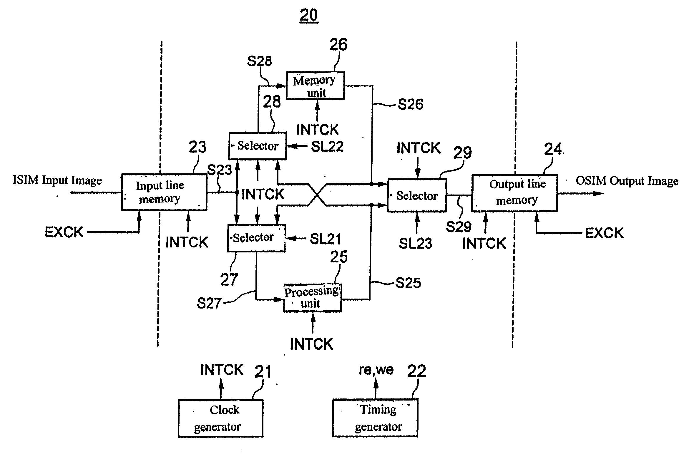
[0061] FIG. 3 is a block diagram illustrating the first embodiment of the image processing device disclosed in the present invention. FIG. 4 is the timing diagram of the image processing device shown in FIG. 3.

[0062] As shown in FIG. 3, the image processing device 20 disclosed in the first embodiment comprises clock generator 21, timing generator 22, input line memory 23, output line memory 24, processing unit 25, memory unit 26, as well as selectors 27, 28, and 29.

[0063] The transfer part comprises selector 27 (first selector) and selector 28 (second selector).

[0064] Clock generator 21 generates an internal clock signal INTCK of several hundred MHz which is n times faster than the external clock (for example, tens of MHz) and supplies this clock signal to the reading system of input line memory 23, the writing system of output line memory 24, the input / output system of processing unit 25, the writing and reading systems of memory unit 26, and various selector...

second embodiment

[0100] Second Embodiment

[0101] FIG. 7 is a block diagram illustrating the second embodiment of the image processing device disclosed in the present invention.

[0102] The difference between the second embodiment and said first embodiment is that the transfer speed between the input / output line memory and the memory unit, the operating speed of the processing unit, and the storage speed of the memory unit are different from each other.

[0103] More specifically, for the image processing device 20A disclosed in the second embodiment, processing unit 25A comprises input buffer 252, output buffer 253, and processing circuit 254. Memory unit 26A comprises input buffer 263, output buffer 264, and memory circuit 265. Said input buffers 252 and 263 as well as output buffers 253 and 264 input / output image data operate synchronously with internal clock signal INTCK generated by clock generator 21 (not shown in FIG. 7). Said processing circuit 254 and memory circuit 265 perform calculation and sto...

third embodiment

[0107] Third Embodiment

[0108] FIG. 8 is a block diagram illustrating the third embodiment of the image processing device disclosed in the present invention.

[0109] The difference between the third and second embodiments is as follows: the memory part has multiple input buffers (two in the third embodiment); as a result, a second input line memory is adopted; during the stage when the first input image ISIM1 input from the first input line memory 23-1 to the first input buffer 263-1 of memory unit 26B and the intermediate processing data between processing unit 25B and memory unit 26B, or the second input image ISIM2, which is asynchronous with the scan line of the data output from processing unit 25B or memory unit 26B to output line memory 24, are input to the second input buffer 263-2 of memory unit 26B from the second input line memory 23-2 and are output from output buffer 264, the second image is synchronized with the first image.

[0110] Although the entire circuit is not shown i...


PUM


Abstract

The objective of the invention is to provide an image processing device that can operate at high speed even if input/output with respect to the outside is performed at low speed, and that can fully exploit processibility, by means of input line memory 23 and output line memory 24, which can store image data of one scan line, and are arranged in the input unit and output unit, respectively; the input image data are written in input line memory 23 at the speed of the input image data; the image data that have been written to the input line memory are read at a speed n times faster than the input image data and are sent to processing unit 25 or memory unit 26; processing unit 25 and memory unit 26 receive the image data of one scan line at a speed n times faster than the speed of the input image data, perform a prescribed processing, and then output the processing results at a speed n times faster than the speed of the input image data; the image data output from processing unit 25 or memory unit 26 are selected by selector 29 and written to output line memory 24 at a speed n times faster than the speed of the input image data; the output image data are read in units of one scan line from output line memory 24 at a prescribed speed.

Description

[0001] The present invention pertains to an image processing device that has a processing unit, that acts as an image processor for processing image data in units of one scan line, and a memory unit that can read and write in units of one scan line.[0002] FIG. 1 is a block diagram illustrating the basic configuration of a conventional image processing device. FIG. 2 is the timing chart of the image processing device shown in FIG. 1.[0003] As shown in FIG. 1, said image processing device 10 comprises processing unit 13, which processes data in units of one scan line, memory unit 14 which can read and write in units of one scan line, and selector 15 which outputs the output data of processing unit 13 or the data read from memory unit 14 in accordance with a selection signal SL1.[0004] Said processing unit 13 comprises an SIMD (single-instruction multiple-data) type image DSP (digital signal processor) which has multiple processor elements (PE) arranged in parallel with each other and ...

Claims


Application Information

Patent Timeline
IPC IPC(8): B41B1/00B41J1/00G06F3/153G06F15/00G06T1/60G06K15/00G06T1/20H04N1/32
CPCG06K15/00H04N1/32358H04N1/32443H04N2201/3287H04N2201/3292
Inventor MIYAGUCHI, HIROSHIKOJIMA, TAKAO
Owner TEXAS INSTR INC
Why Eureka
Try Eureka