

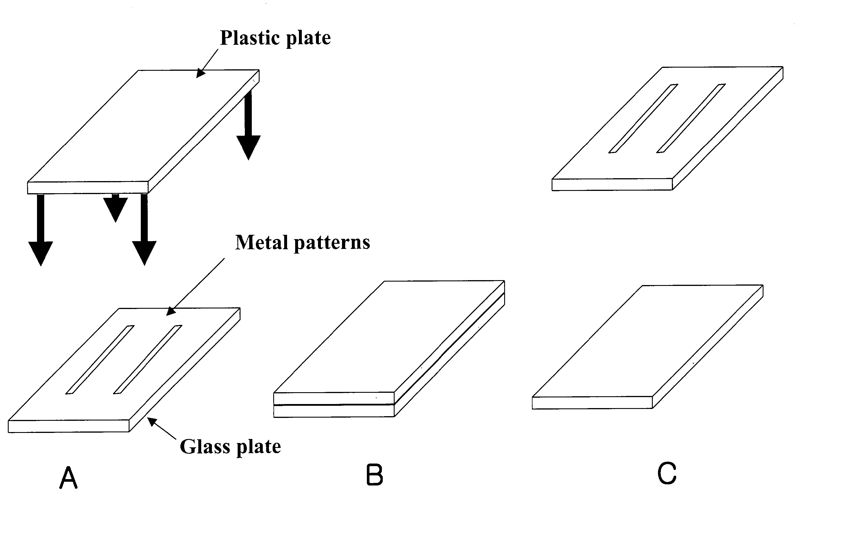
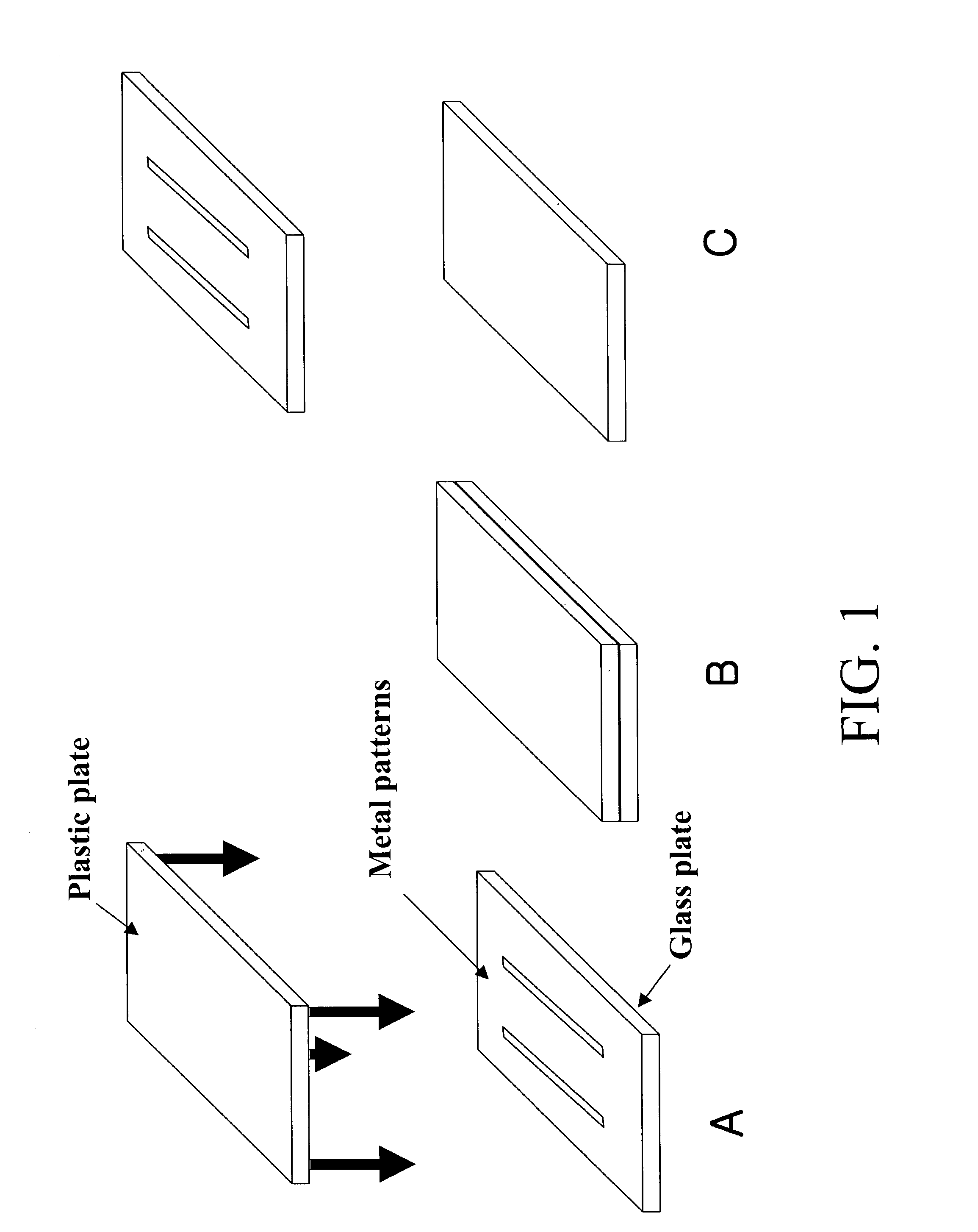
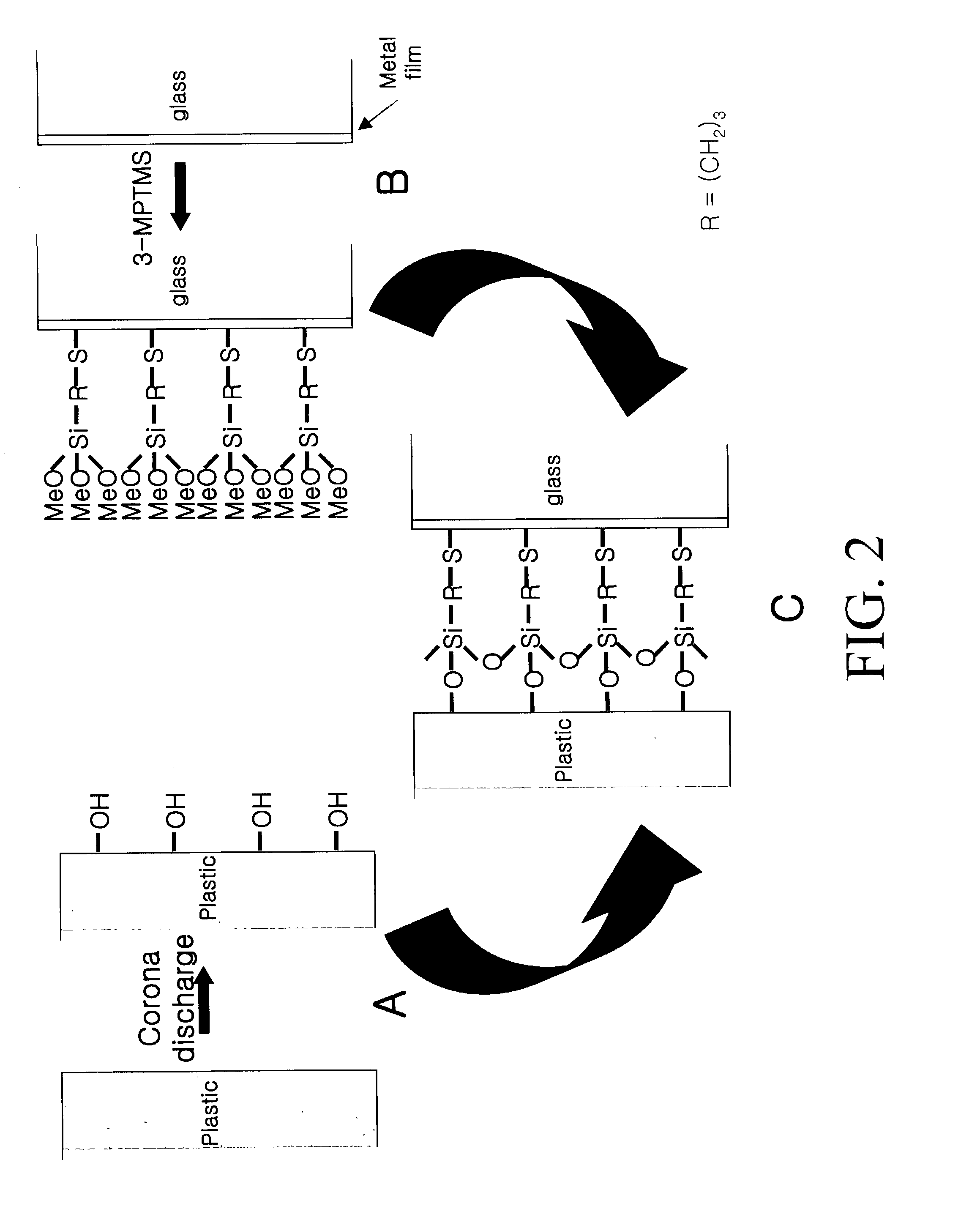
Process for forming metal micro-patterns on plastic substrate
a technology of plastic substrate and metal micro-pattern, which is applied in the direction of printed circuit secondary treatment, chemical vapor deposition coating, precision positioning equipment, etc., can solve the problems of difficult to control the thickness or reduce the line width of the micro-pattern, and difficult to fabricate a plastic lab-on-a-chip system
- Summary
- Abstract
- Description
- Claims
- Application Information
AI Technical Summary
Problems solved by technology
Method used
Image

Examples
example 2
[0044] A plastic lab-on-a-chip for an electrochemical detector was fabricated as follows;
[0045] Referring to FIG. 6, "A" is a PDMS plate having micro-channels prepared by a conventional replica molding method, "B" is a PDMS plate having two Au electrodes and a Ag electrode prepared as in Example 1. The surfaces of the "A" and "B" plates were treated with corona discharge, and the two plates were combined to obtain a plastic lab-on-a-chip ("C").
[0046] FIG. 7 illustrates a microscopic image of the gold and silver metal pattern aligned with PDMS microchannel. The channel size was 100 .mu.m wide and 30 .mu.m deep, and the electrodes, each 50 .mu.m wide and 200 nm thick, were spaced at an interval of 100 .mu.m. The resistance of the electrode was 60 .OMEGA., and the electric conductivity measured when the channel was filled with 10 mM NaCl aqueous solution was about 1.6 S.
[0047] Reservoirs for providing and receiving samples were connected to the channel terminals, to fabricate a plastic...
PUM
| Property | Measurement | Unit |
|---|---|---|
| Molar density | aaaaa | aaaaa |
| Electrical conductivity | aaaaa | aaaaa |
| Electrical conductor | aaaaa | aaaaa |
Abstract
Description
Claims
Application Information