Multilayer ceramic substrate and method for manufacturing the same

a multi-layer ceramic and substrate technology, applied in the field of multi-layer ceramic substrates, can solve the problems of difficult to produce a large flat substrate, and difficult to produce a substrate with high dimensional accuracy

a multi-layer ceramic and substrate technology, applied in the field of multi-layer ceramic substrates, can solve the problems of difficult to produce a large flat substrate, and difficult to produce a substrate with high dimensional accuracy

US20030094307A1Inactive Publication Date: 2003-05-22PANASONIC CORP

Image

  • Multilayer ceramic substrate and method for manufacturing the same
  • Multilayer ceramic substrate and method for manufacturing the same
  • Multilayer ceramic substrate and method for manufacturing the same

Examples


example 1

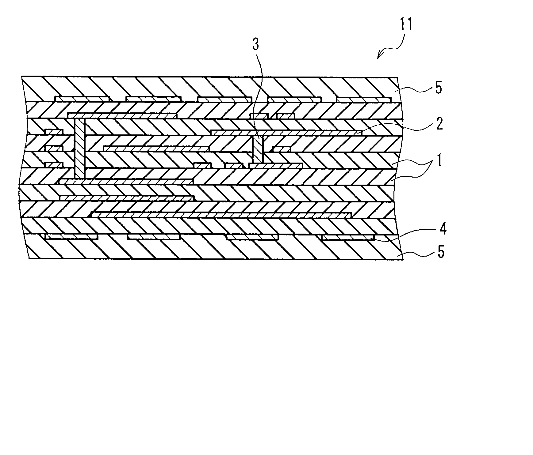
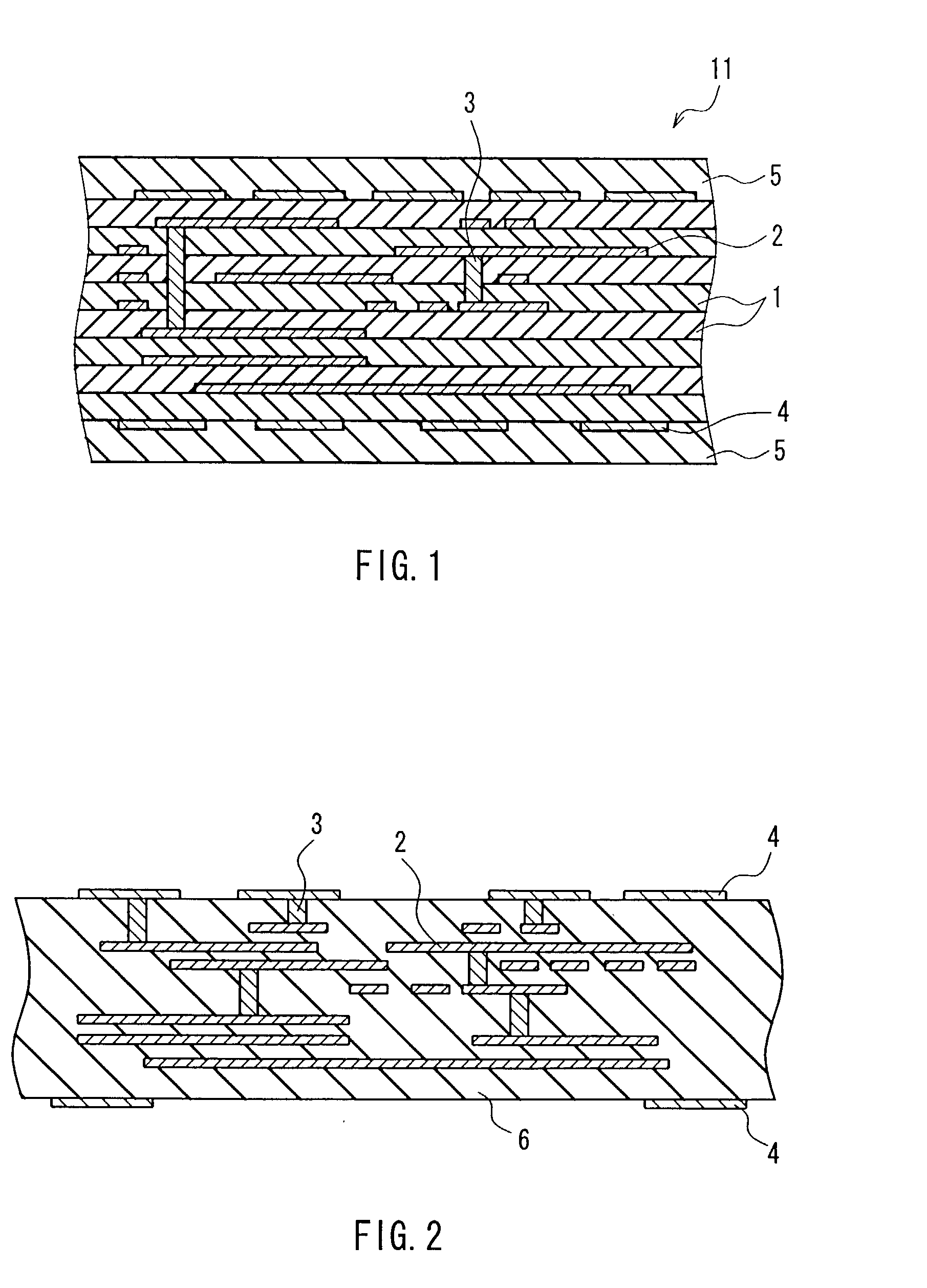
[0048] A multilayer ceramic substrate of the above embodiment was produced and evaluated with actual measurement. In this example, the multilayer ceramic substrates were produced by using conductor compositions that differ in conductive powder or Mo compound, and then the electrode and the ceramic body of each of the multilayer ceramic substrates were evaluated. Table 1 shows the results. The conductor compositions in Example 1 did not include a glass frit.

1TABLE 1 Average Amount of Mo State in particle Amount of compound in the Conductor Conductive diameter glass frit terms of Mo vicinity of resistance No. powder (.mu.m) (wt part) metal (wt part) electrode (.times. 10.sup..multidot.6 .OMEGA.cm) Comparative Ag 3 0 0 defective 1.8 example 1 Ag 3 0 MoO.sub.3 0.075 good 1.8 (Mo: 0.05) 2 Ag 3 0 MoO.sub.3 1.5 good 2.0 (Mo: 1) 3 Ag 3 0 MoO.sub.3 3 good 2.2 (Mo: 2) 4 Ag 3 0 MoO.sub.3 3.75 good 2.5 (Mo: 2.5) 5 Ag 3 0 MoO.sub.3 4.5 good 4.0 (Mo: 3) 6 Ag 3 0 MoO.sub.3 7.5 good 4.9 (Mo: 5) 7 A...

example 2

[0055] Multilayer ceramic substrates were produced by using conductor compositions that differ in the softening point and the amount of a glass frit, and then the electrode and the ceramic body of each of the multilayer ceramic substrates were evaluated in the same manner as Example 1. Table 2 shows the results.

2TABLE 2 Softening Average point and Amount of Mo State in particle amount of compound in the Conductor Conductive diameter glass frit terms of Mo vicinity of resistance No. powder (.mu.m) (wt part) metal (wt part) electrode (.times.10.sup..multidot.6 .OMEGA.cm) 17 Ag 3 450.degree. C. MoO.sub.3 3.75 defective 2.6 3.0 (Mo: 2.5) 18 Ag 3 580.degree. C. MoO.sub.3 3.75 defective 2.7 3.0 (Mo:2.5) 19 Ag 3 670.degree. C. MoO.sub.3 3.75 good 2.5 3.0 (Mo: 2.5) 20 Ag 3 780.degree. C. MoO.sub.3 3.75 good 2.6 3.0 (Mo: 2.5) 21 Ag 3 850.degree. C. MoO.sub.3 3.75 good 2.5 3.0 (Mo:2.5) 22 Ag 3 780.degree. C. MoO.sub.3 3.75 good 4.2 5.0 (Mo: 2.5) 23 Ag 3 780.degree. C. MoO.sub.3 3.75 good 5.1 ...


PUM

PropertyMeasurementUnit
softening pointaaaaaaaaaa
thicknessaaaaaaaaaa
particle diameteraaaaaaaaaa

Abstract

A multilayer ceramic substrate includes a glass ceramic body, a conductive pattern, and a via conductor. The conductive pattern is formed in the glass ceramic body and on at least one principal surface of the glass ceramic body. The via conductor makes a connection between the predetermined conductive patterns. The via conductor includes a conductive material and a Mo compound or a Mo metal. The conductive material includes at least one selected from the group consisting of Ag, Au, Pt and Pd as a main component. The amount of Mo compound or Mo metal is in the range of 0.05 to 10 parts by weight in terms of Mo metal with respect to 100 parts by weight of the conductive material. This multilayer ceramic substrate can achieve sufficient flatness and high dimensional accuracy, while preventing defects that occurs in the vicinity of electrodes after firing.

Description

[0001] 1. Field of the Invention[0002] The present invention relates to a multilayer ceramic substrate used for a high-density multilayer circuit substrate.[0003] 2. Description of the Related Art[0004] A multilayer ceramic substrate produced by firing at low temperatures (hereinafter, referred to as a multilayer ceramic substrate) is used for a high-density circuit substrate. The multilayer ceramic substrate is produced by stacking a plurality of ceramic green sheets, each of which has a conductive pattern formed by a conductor composition, and firing the laminate of the ceramic green sheets. To connect the conductive pattern of one layer to that of the other layer, through holes (via holes) are formed in the green sheet of the desired layer beforehand, and then conductor paste (i.e., the conductor composition) is filled into the via holes. Thereafter, the laminate that includes the green sheet having the through holes filled with the conductor paste is fired. In this manner, the g...

Claims


Application Information

Patent Timeline
22 May 2003
Publication
US20030094307A1
IPC
H01L23/498; H05K1/09; H05K3/40
CPC
H01L23/49827; H01L23/49883; H01L2924/09701; H05K1/092; Y10T428/24926; H05K3/4629; H01L2924/0002; H05K3/4061
Inventors
SAITO, RYUICHI; KATSUMURA, HIDENORI