Semiconductor device and manufacturing method thereof

a technology of semiconductors and semiconductors, applied in the direction of semiconductor devices, electrical devices, transistors, etc., can solve the problems of short circuit between bit lines in the memory cell region, no practical influence, and wet etching cannot secure the selectivity of metal silicid

Inactive Publication Date: 2003-06-12
FUJITSU LTD
View PDF0 Cites 2 Cited by
  • Summary
  • Abstract
  • Description
  • Claims
  • Application Information

AI Technical Summary

Problems solved by technology

This is because wet etching cannot secure selectivity to metal silicide.
When the oxide film removing processing is performed by the dry etching, it is required that the metal silicide is always formed on a base in which the contact holes are formed, since selectivity to a substrate cannot be secured and damage to the substrate cannot b

Method used


Image

  • Semiconductor device and manufacturing method thereof
  • Semiconductor device and manufacturing method thereof
  • Semiconductor device and manufacturing method thereof

Examples


first embodiment

[0110] A manufacturing method of an SONOS-type flash memory in which siliciding is performed by a conventional method is shown as a comparison example of the present invention. Note that the same reference numerals and symbols are used to designate the same components and so on as those explained in the first embodiment, and therefore, the explanation thereof will be omitted.

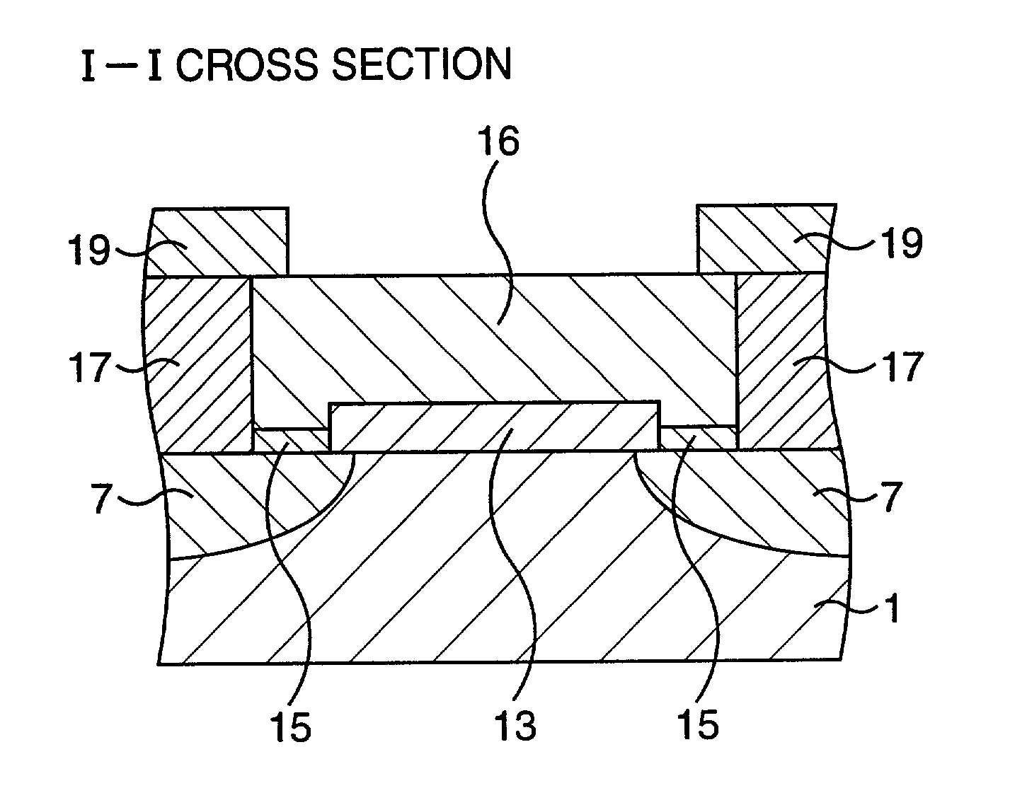
[0111] FIG. 9 and FIG. 10 are diagrammatic plan views showing major processes of the conventional manufacturing method of the SONOS-type flash memory, and FIG. 11A and FIG. 11B are diagrammatic cross-sectional views of the same.

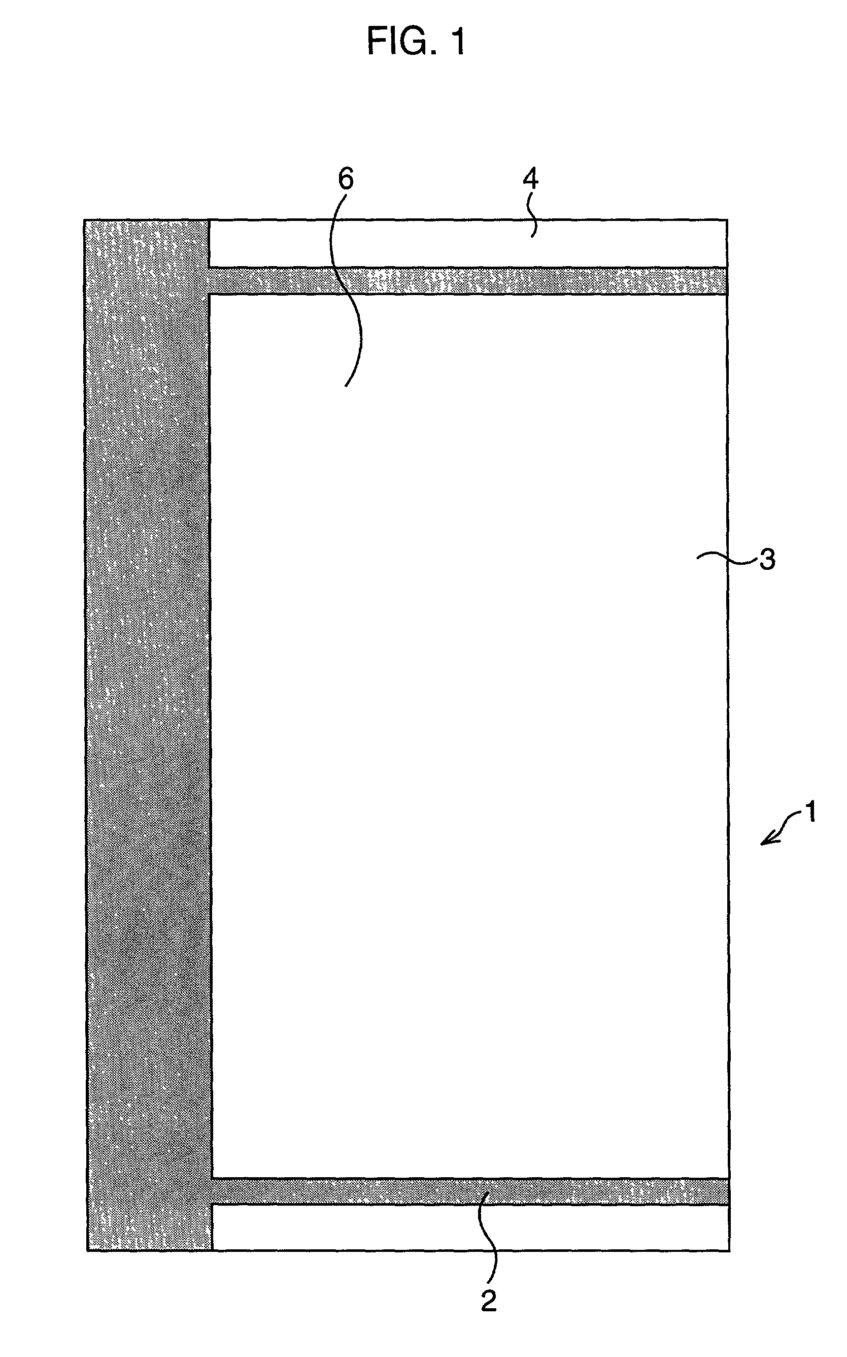
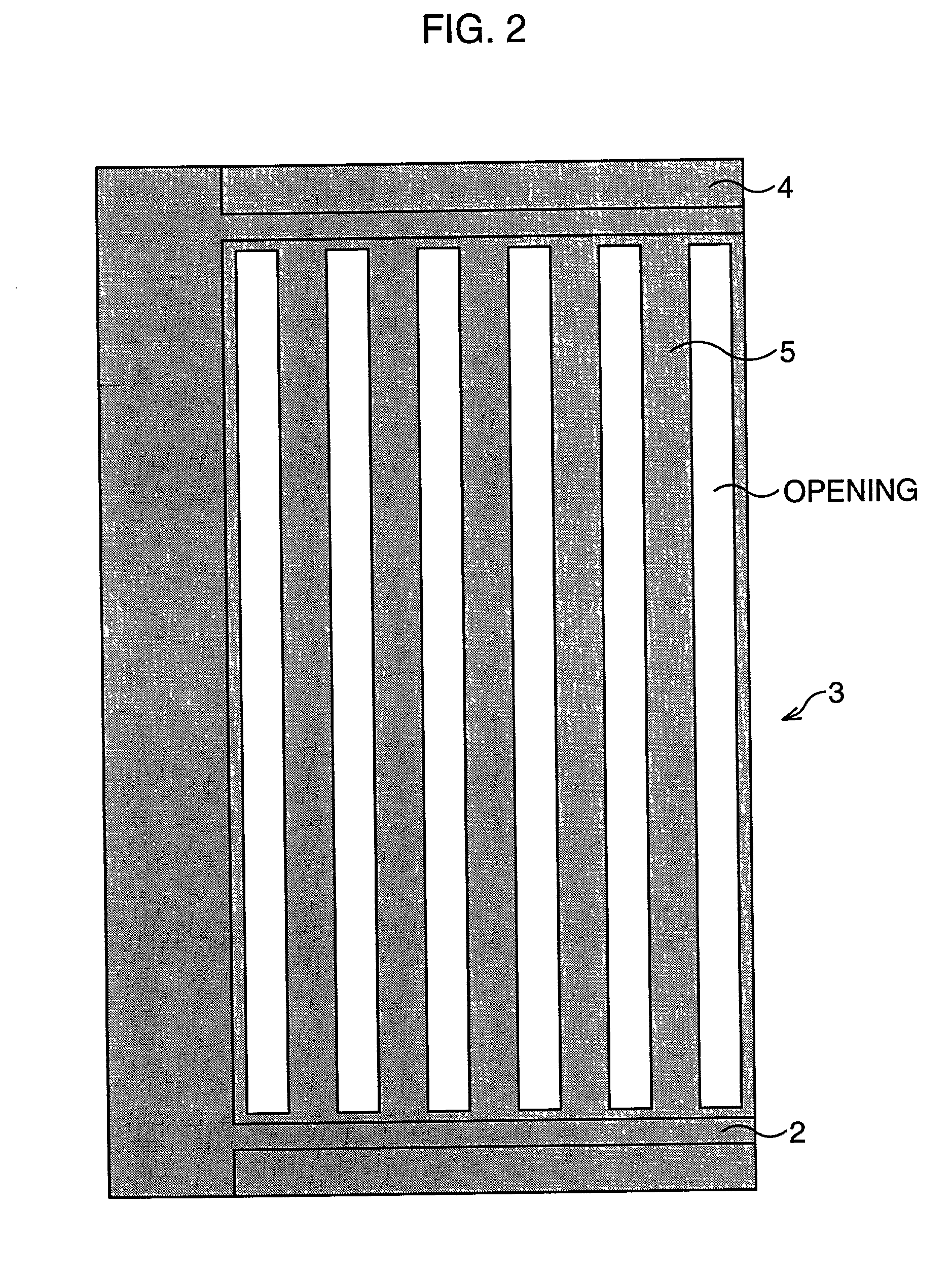
[0112] After each process in FIG. 1 to FIG. 4 similarly to the above-described first embodiment, a silicon oxide film is first deposited on the entire surface by a CVD method. This silicon oxide film is full-anisotropically etched. Thereby, as shown in FIG. 9, side walls 114 are formed on the side walls of the word lines 8 in the active region 3 of the memory cell. In the active region 4 ...

second embodiment

[0116] Next, a second embodiment of the present invention will be explained. A manufacturing method of an SONOS-type flash memory in this second embodiment is substantially the same as that in the first embodiment. However, it is different in the shape of the guard film at the time when the bit lines are silicided. Note that the same reference numerals and symbols are used to designate the same components and so on as those explained in the first embodiment, and therefore, the explanation thereof will be omitted.

[0117] FIG. 12 and FIG. 13 are diagrammatic plan views showing major processes of the manufacturing method of the SONOS-type flash memory according to the second embodiment, and FIG. 14 is a diagrammatic cross-sectional view of the same.

[0118] After each process in FIG. 1 to FIG. 3 similarly to the above-described first embodiment, a silicon oxide film is first deposited on the entire surface by a CVD method. Thereafter, as shown in FIG. 12, on this silicon oxide film, a lat...

third embodiment

[0132] Next, a third embodiment of the present invention will be explained. A manufacturing method of an SONOS-type flash memory in this third embodiment is substantially the same as that in the first embodiment. However, it is different in the shape of the guard film at the time when the bit lines are silicided. Note that the same reference numerals and symbols are used to designate the same components and so on as those explained in the first embodiment, and therefore, the explanation thereof will be omitted.

[0133] FIG. 16 and FIG. 17 are diagrammatic plan views showing major processes of the manufacturing method of the SONOS-type flash memory according to the third embodiment, and FIG. 18A and FIG. 18B are diagrammatic cross-sectional views of the same.

[0134] After each process in FIG. 1 to FIG. 3 similarly to the above-described first embodiment, a silicon oxide film is first deposited on the entire surface by a CVD method. Thereafter, as shown in FIG. 16, on this silicon oxide ...


PUM


Abstract

A resist pattern is formed on a silicon oxide film. This resist pattern is formed in such a shape to expose only portions necessary for electrical insulation between bit lines adjacent to each other. In other words, here, these portions are a connection hole forming region in which a contact hole of the bit line is formed and a connection hole forming region in which a contact hole of a word line is formed. Using this resist pattern as a mask, an insulation region is formed by full anisotropic etching of the silicon oxide film. Siliciding is performed in this state and silicide is formed on a surface of the bit line exposed to the connection hole forming region and a surface of a source/drain in an active region of a peripheral circuit.

Description

[0001] This application is based upon and claims priority of Japanese Patent Application No. 2001-374840, filed on Dec. 7, 2001, the contents being incorporated herein by reference.[0002] 1. Field of the Invention[0003] The present invention relates to a semiconductor device and a manufacturing method thereof in which bit lines are formed of an impurity diffused layer and word lines are formed to cross the bit lines via an insulation film having a charge-capture function or a floating gate.[0004] 2. Description of the Related Art[0005] Conventionally, as a nonvolatile memory which retains stored information even when a power source is cut off, such a semiconductor memory has been invented in which an impurity diffused layer formed on a semiconductor substrate forms bit lines (embedded bit lines), and word lines are formed on the semiconductor substrate via a capacity insulation film to cross the bit lines at right angles. Furthermore, semiconductor memories adaptable to further down...

Claims


Application Information

Patent Timeline
IPC IPC(8): H01L21/8246H01L21/8247H01L27/10H01L27/115H01L29/788H01L29/792
CPCH01L27/115H01L27/11521H01L27/11568H01L27/11531H01L27/11526H10B41/42H10B41/40H10B69/00H10B41/30H10B43/30H01L27/10H10B99/00
Inventor TAKAHASHI, KOJIYOSHIMURA, TETSUO
Owner FUJITSU LTD
Why Eureka
Try Eureka