Method of forming a self-aligned floating gate in flash memory cell

a floating gate and flash memory technology, applied in the direction of semiconductors, electrical devices, transistors, etc., can solve the problems of memory cell program and erase failure, poor uniformity of wafers, and difficulty in implementing uniform floating gates, etc., to achieve the effect of reducing spacing

Inactive Publication Date: 2003-06-26
SK HYNIX INC
View PDF0 Cites 16 Cited by
  • Summary
  • Abstract
  • Description
  • Claims
  • Application Information

AI Technical Summary

Benefits of technology

0006] Methods are disclosed which prevent generation of a moat in a trench insulating film and to minimize spacing of a floating gate to be formed in a subsequent process...

Problems solved by technology

During the process of isolating a floating gate using a mask patterning, wafer uniformity is poor because of variations in the critical dimension (CD).
It is thus difficult to implement a uniform floating gate.
Further, there are problems such as program and erase fail of the memory cell, or the like, as a result of variations in the coupling ratio.
In addition, when a space of below 0.13 .mu.m is implemented in a highly-integrated design, the mask process is made more difficult.
Thus, the process of manufacturing the flash memory cell serving as an important factor in implementing a uniform floating gate is made more...

Method used


Image

  • Method of forming a self-aligned floating gate in flash memory cell
  • Method of forming a self-aligned floating gate in flash memory cell
  • Method of forming a self-aligned floating gate in flash memory cell

Examples


Embodiment Construction

[0012] The disclosed methods will be described in detail by way of a preferred embodiment with reference to accompanying drawings.

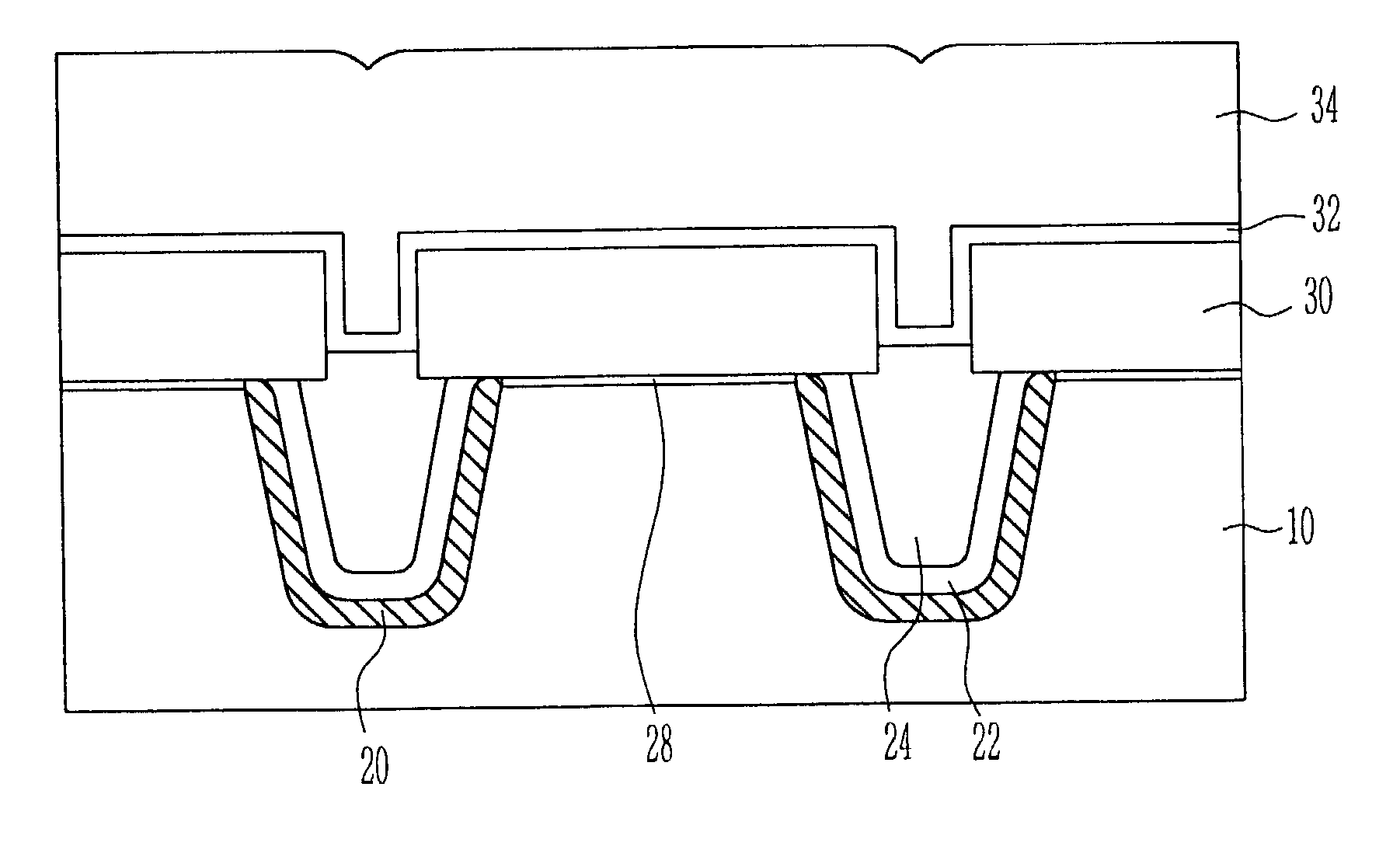
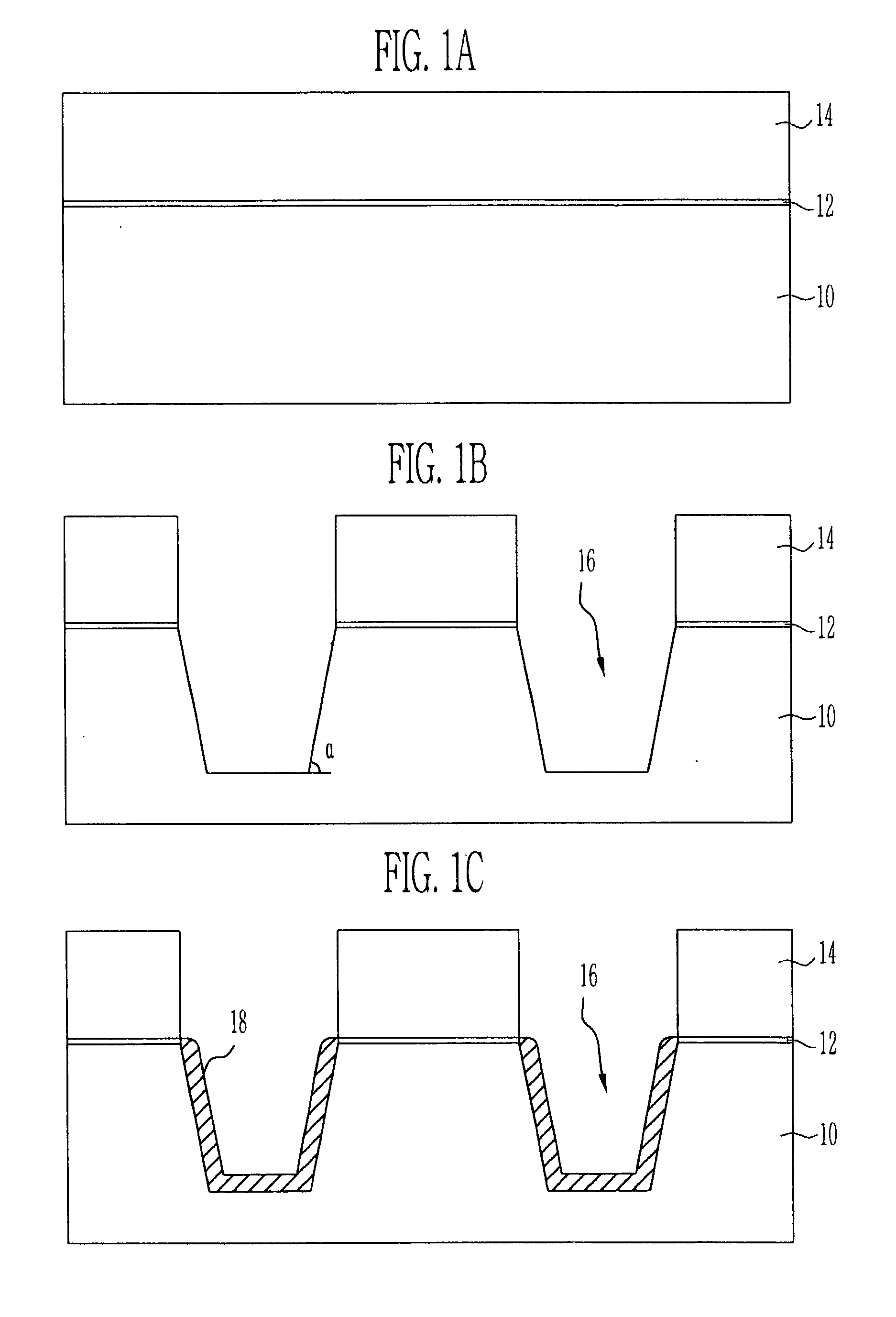
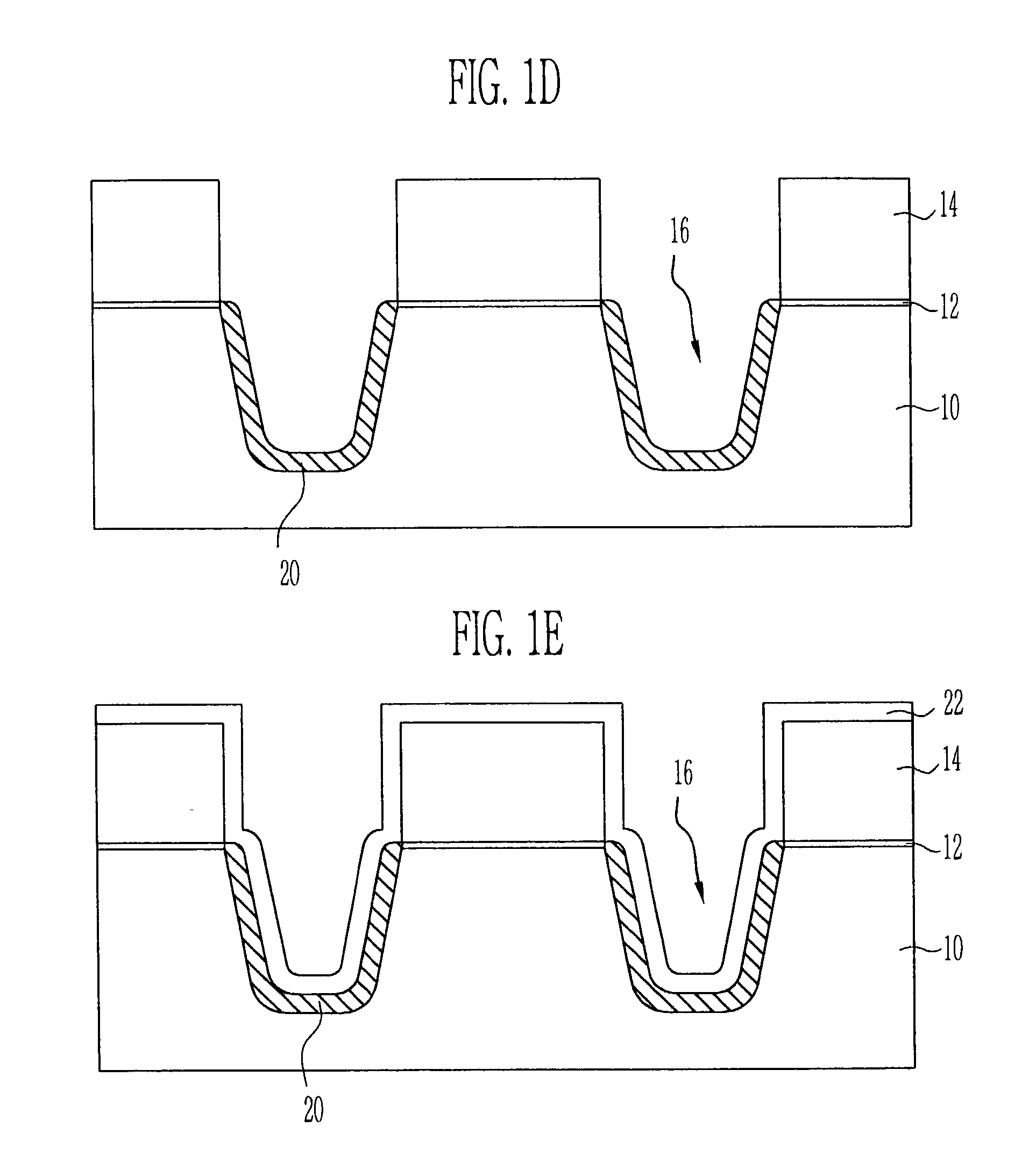
[0013] FIG. 1A to FIG. 1K are cross-sectional views of self-aligned floating gates in a flash memory cell for describing a method of the floating gate according to a preferred embodiment of the disclosed methods.

[0014] Referring now to FIG. 1A, a semiconductor substrate 10 is cleaned by a pre-processing cleaning process. Next, a pad oxide film 12 and a pad nitride film 14 are sequentially formed on the semiconductor substrate 10. At this time, the preprocessing cleaning process is performed using diluted HF (DHF, typically a HF solution into which H.sub.2O is diluted at the ratio of about 50:1) or buffer oxide etchant (BOE, which is a solution in which HF and NH.sub.4F are mixed at the ratio ranging from about 100:1 to about 300:1).

[0015] Further, the pad oxide film 12 is formed by dry or wet oxidization process at a given temperature in order to remove c...


PUM


Abstract

A method of forming a self-aligned floating gate in a flash memory cell. A capping layer is formed on a trench insulating film. An etching process is then performed to etch the trench insulating film to a desired dimension. Therefore, generation of a moat in the trench insulating film is avoided. Further, spacing of a floating gate formed in a subsequent process can be minimized.

Description

[0001] 1. Technical Field[0002] A method of forming a self-aligned floating gate in a flash memory cell is disclosed. More specifically, a method of forming a trench insulating film is disclosed which is capable of preventing formation of a moat that is generated when the self-aligned floating gate is formed in the flash memory cell.[0003] 2. Description of the Related Art[0004] Generally, a flash memory cell is fabricated using shallow trench isolation (STI) as a device isolation process. During the process of isolating a floating gate using a mask patterning, wafer uniformity is poor because of variations in the critical dimension (CD). It is thus difficult to implement a uniform floating gate. Further, there are problems such as program and erase fail of the memory cell, or the like, as a result of variations in the coupling ratio. In addition, when a space of below 0.13 .mu.m is implemented in a highly-integrated design, the mask process is made more difficult. Thus, the process...

Claims


Application Information

Patent Timeline
IPC IPC(8): H01L21/28H01L21/768H01L21/8247H01L27/115H01L29/423H01L29/788H01L29/792
CPCH01L21/28273H01L27/11521H01L27/115H01L29/40114H10B69/00H10B41/30
Inventor JEONG, CHEOL MOSOHN, PYENG GEUN
Owner SK HYNIX INC
Why Eureka
Try Eureka