
Stacked semiconductor package

Inactive Publication Date: 2003-07-10
KK TOSHIBA
View PDF3 Cites 26 Cited by
  • Summary
  • Abstract
  • Description
  • Claims
  • Application Information

AI Technical Summary

Problems solved by technology

A high temperature of a semiconductor chip harmfully affects operations and reliability of the semiconductor device.
Particularly in a semiconductor memory such as a dynamic random access read write memory (DRAM), a high temperature causes deterioration in memory retention characteristics.

Method used


Image

  • Stacked semiconductor package
  • Stacked semiconductor package
  • Stacked semiconductor package

Examples


first embodiment

[0018] (First Embodiment)

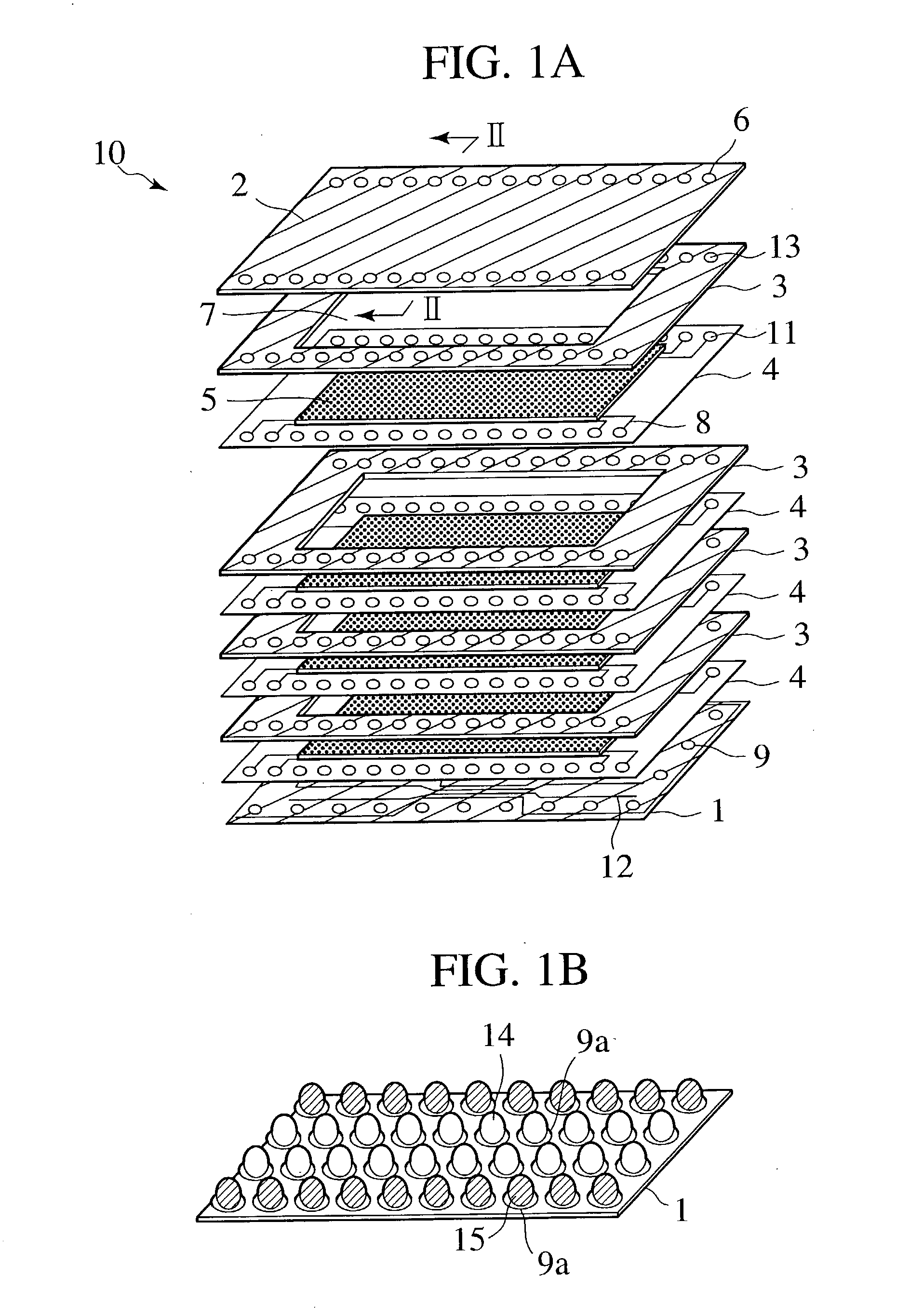
[0019] FIG. 1A shows a structure of an SBM-type semiconductor package according to a first embodiment.

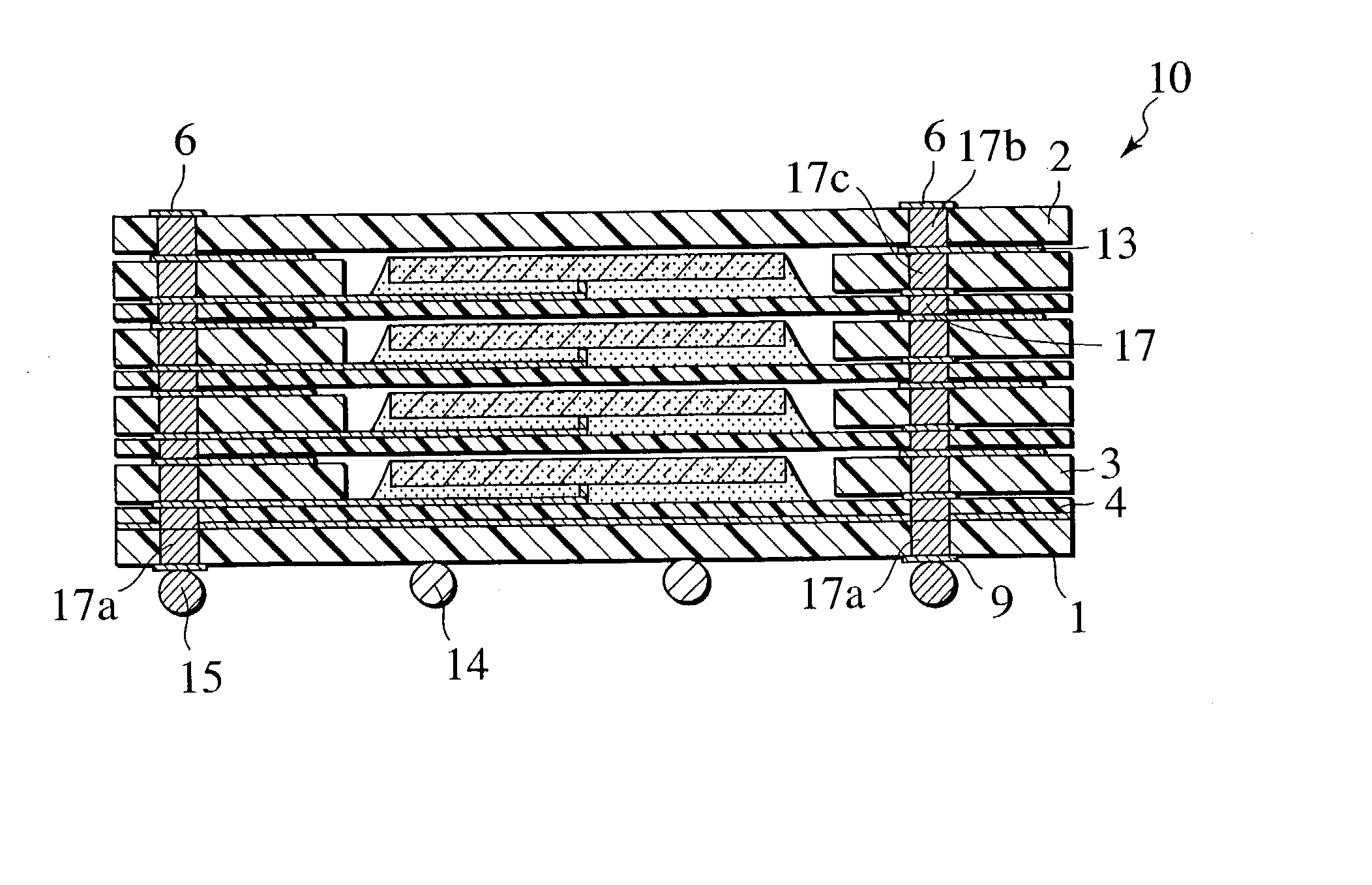
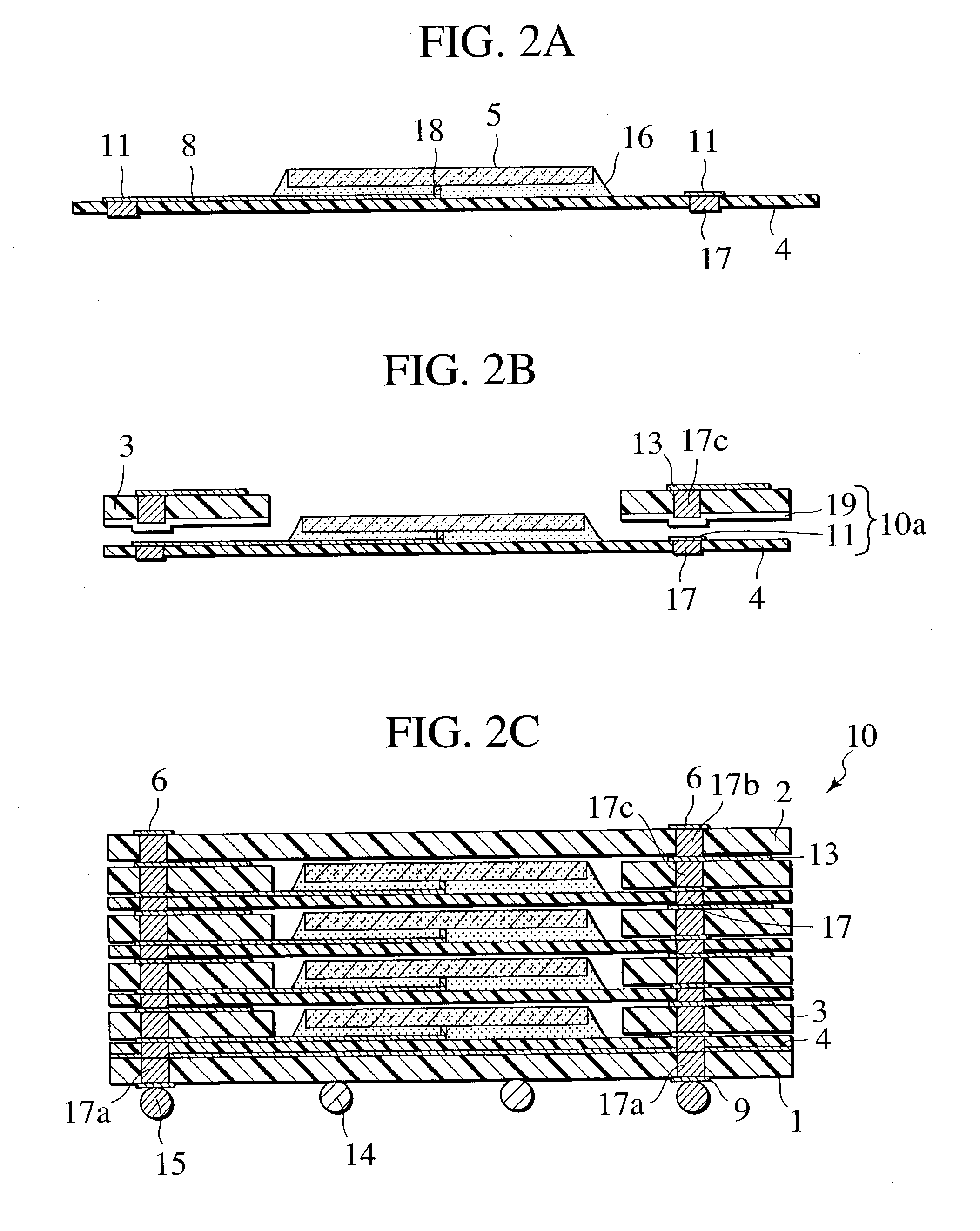
[0020] The semiconductor package 10 according to the first embodiment includes circuit boards 4 each having a semiconductor chip 5 mounted thereon, a first insulating substrate 1 which has external connection terminal balls 14 (first electrically conductive balls) which is placed at the bottom of the package, a second insulating substrate 2 which seals the package and which is placed at the top of the package, and third insulating substrates 3 each having a chip cavity 7 for housing the semiconductor chip 5. Specifically, as shown in FIG. 1A and FIGS. 2A to 2C, in the semiconductor package 10, a plurality of semiconductor chip units 10a, each having a structure in which the frame-shaped third insulating substrate 3 having the chip cavity 7 is mounted on the circuit board 4 having the semiconductor chip 5 mounted thereon, are stacked. The stack is sandwiched ...

second embodiment

[0040] (Second Embodiment)

[0041] FIG. 5 is a cross-sectional view of an SBM-type stacked semiconductor package according to a second embodiment. In the second embodiment, although four semiconductor (such as silicon) devices (chips) are stacked, the number of semiconductor chips to be stacked is not limited. A required number, of two or more, semiconductor chips are stacked..

[0042] In the semiconductor package 20 according to the second embodiment, a plurality of units, each having a structure in which a frame-shaped third insulating substrate 23 having a chip cavity 7 is mounted on a circuit board 24 having a semiconductor chip 25 mounted thereon and in which a heat conductive resin layer 30 covers the semiconductor chip 25, are stacked. The stack is sandwiched by first and second insulating substrates 21 and 22, and then the resultant structure is heated and pressed to be made monolithic, thus forming the semiconductor package 20.

[0043] Similarly to the semiconductor package 10 ac...

third embodiment

[0056] (Third Embodiment)

[0057] FIG. 6 is a cross-sectional view of a semiconductor apparatus in which an SBM-type semiconductor package is mounted on a mount board. A semiconductor package 25 having a similar structure to that of the first or second embodiment is mounted on the mount board 31, for example.

[0058] As the mount board 31, a circuit board having multilayer wiring of 6 layers impregnated with epoxy resin, is used, for example. Concerning the multilayer wiring buried in the circuit board, signal wiring 39 is located on the uppermost layer, and is followed by power supply wiring 39a, signal wiring 39 and 39, ground wiring 39b, and signal wiring 39, which are located in this order in a multilayered manner. The power supply wiring 39a and the ground wiring 39b are connected to beat conducting paths 38 and 38a made of aluminum or the like, one ends of which are exposed on a surface of the mount board. The heat conducting paths 38 and 38a are exposed on the surface of the moun...


PUM


Abstract

A semiconductor package includes a first insulating substrate, a second insulating substrate, and a plurality of semiconductor chip units placed between the first and second insulating substrates. The first insulating substrate has wiring placed on one surface thereof and has first electrically conductive balls which are used as external connection terminals and second electrically conductive balls which radiate heat. The first and second electrically conductive balls are on the other surface thereof. The second insulating substrate is placed opposite to the one surface of the first insulating substrate. Each semiconductor chip unit has a semiconductor chip; a circuit board which has the semiconductor chip mounted thereon and wiring electrically connected to terminals of the semiconductor chip; and a third insulating substrate which is placed on the circuit board and which has a chip cavity for housing the semiconductor chip. By use of the second electrically conductive balls placed on the first insulating substrate, beat generated in the semiconductor chip is efficiently released outside, thus preventing an increase in temperature of the semiconductor chip.

Description

[0001] This application is based upon and claims the benefit of priority from the prior Japanese Patent Application No. 2002-000069 filed on Jan. 4, 2002, the entire contents of which are incorporated herein by reference.[0002] 1. Field of the Invention[0003] The present invention relates to a heat radiation structure of a semiconductor package having a structure in which a plurality of semiconductor chips are stacked.[0004] 2. Description of the Related Art[0005] Semiconductor apparatuses have come to be used in a state where semiconductor chips are stacked in order to increase packaging densities, in many cases. Conventional stacked packages are described in Japanese Patent Publications H9-219490 (published in 1997), H10-135267 (published in 1998), and H10-163414 (published in 1998). In these conventional packages, packages, such as thin small outline packages (TSOPs), tape carrier packages (TCPs), or ball grid arrays (BGAs), are assembled completely, and then the packages, which ...

Claims


Application Information

Patent Timeline
IPC IPC(8): H01L25/065H01L25/10H01L25/11H01L25/18
CPCH01L25/0657H01L2224/16H01L2225/0652H01L2225/06541H01L2225/06572H01L2225/06586H01L2924/10253H01L2225/06593H01L2924/15311H01L2924/01019H01L2924/00H01L2924/1627
Inventor ETO, JUNYAHAYASHI, KIYOTAKA
Owner KK TOSHIBA
Learn More