

Method for manufacturing organic EL device with protective layer
- Summary
- Abstract
- Description
- Claims
- Application Information
AI Technical Summary
Benefits of technology
Problems solved by technology
Method used
Image

Examples
first embodiment
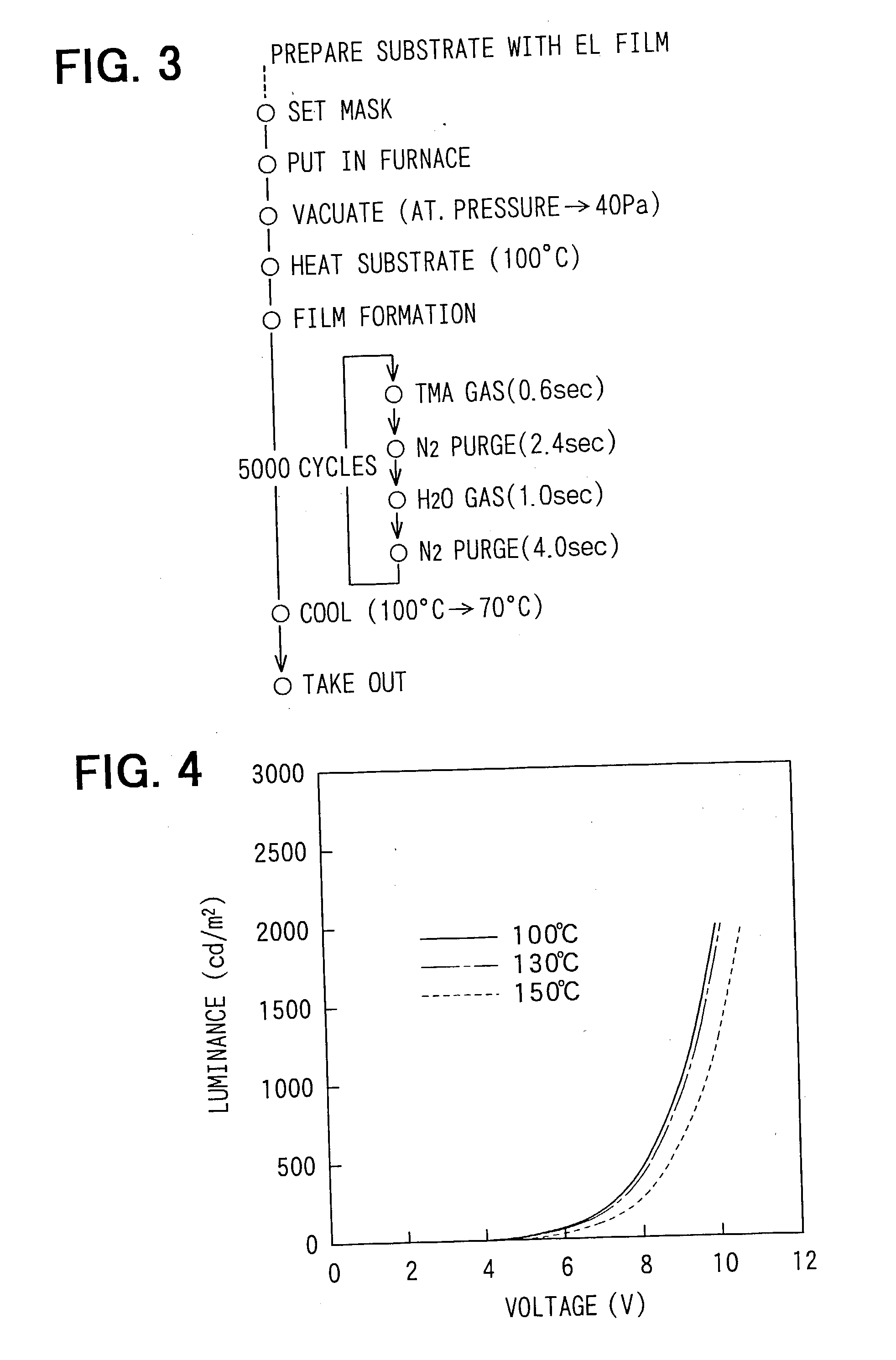
[0107] Accordingly, an Al.sub.2O.sub.3 film of about 320 nm in thickness was obtained as the protective layer 6. The total stress of the protective layer (Al.sub.2O.sub.3+Al.sub.2O.sub.3) 6 of this example was confirmed to be tensile stress of about 140 MPa as shown in FIG. 11 from the deformation (warpage amount) of the glass substrate 1 before and after the film formation. It was also confirmed that the stress is low as compared to the single Al.sub.2O.sub.3 film (the protective layer formed by the process shown in FIG. 3) shown in the
[0108] Therefore, in the organic EL device 100 to which the first example is applied, the protective layer 6 can be composed of laminated films made of the same constituent elements and having different characteristics by changing the film forming conditions. Accordingly, the stress relaxing film and the non-stress relaxing film can be formed relatively. In the first example described above, the Al.sub.2O.sub.3 film formed at first at the substrate t...
second example
[0110] In the second example, films for constituting the protective layer 6 are formed to have different film characteristics from each other by forming them from different constituent elements from each other. FIG. 12 is a flowchart showing a process for forming the protective layer 6 in this example. Specifically, the glass substrate 1 (35 mm.times.45 mm) after cleaning was put into a reaction furnace. The reaction furnace was vacuumed to about 40 Pa and the glass substrate 1 was heated while flowing N.sub.2 gas at about 400 sccm to stabilize the substrate temperature at 130.degree. C.
[0111] Then, SiCl.sub.4 and H.sub.2O were gasified within source material bottles and were introduced to the reaction furnace alternately by N.sub.2 gas (flow rate of 400 sccm) functioning as carrier gas as follows. That is, after introducing gasified SiCl.sub.4 for 1.0 second, N.sub.2 gas was introduced for 2.4 seconds. After that, gasified H.sub.2O was introduced for 3.0 seconds and N.sub.2 purge g...
fourth embodiment
[0117] (Fourth Embodiment)
[0118] FIG. 14 shows a partial sectional structure of an organic EL device 200 according to a fourth embodiment of the invention. Although the protective layer 6 is formed only by the ALE method in each embodiment described above, the present embodiment is characterized in that the protective layer 6 is composed of a layer (called an ALE layer) 6a formed by the ALE method and a layer (called a non-ALE layer) 6b formed by a method different from the ALE method.
[0119] In the present embodiment, the protective layer 6 is formed by alternately laminating the ALE layer 6a made of Al.sub.2O.sub.3 of several nm to several tens nm in thickness, and the non-ALE layer 6b made of Al.sub.2O.sub.3 made of several nm to several tens nm in thickness and formed by the CVD method. Here, the ALE layer 6a is formed right above the structures 2 to 5 and the non-ALE layer 6b is formed on the ALE layer 6a. Then, the layers 6a, 6b are laminated alternately thereafter. Although FI...
PUM
 Abstract
Description
Claims
Application Information