

Photoelectric conversion element and photoelectric conversion device
a conversion device and photoelectric technology, applied in the field of photoelectric conversion elements and photoelectric conversion devices, can solve the problems of inapplicability to light, inability to obtain high speed response in several hundreds of ghz bands or several thz, and the upper limit of the speed is about several tens of ghz
- Summary
- Abstract
- Description
- Claims
- Application Information
AI Technical Summary
Benefits of technology
Problems solved by technology
Method used
Image

Examples
example 1
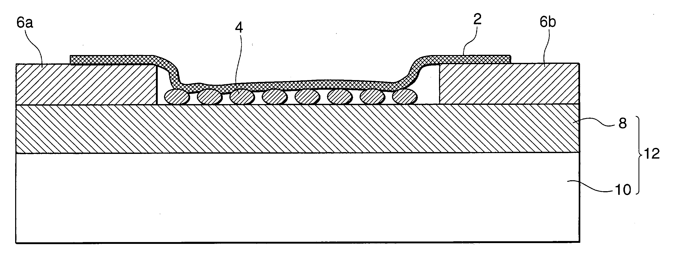
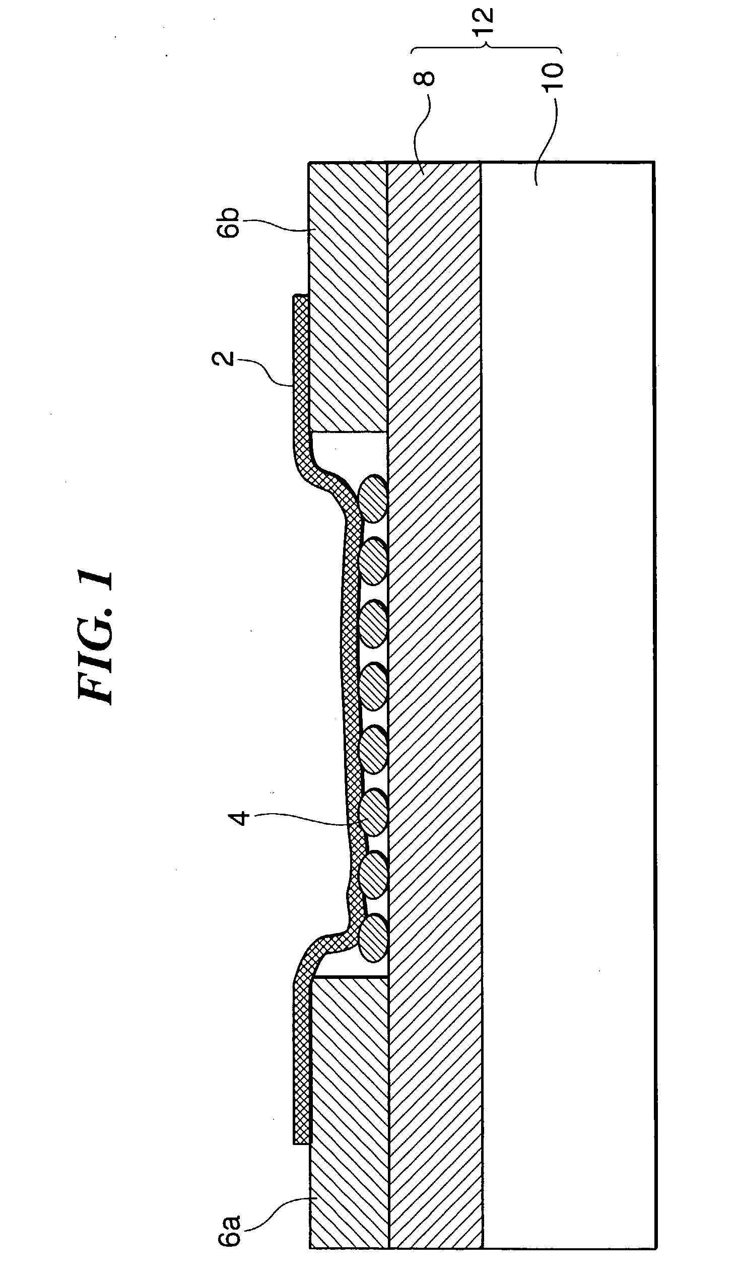
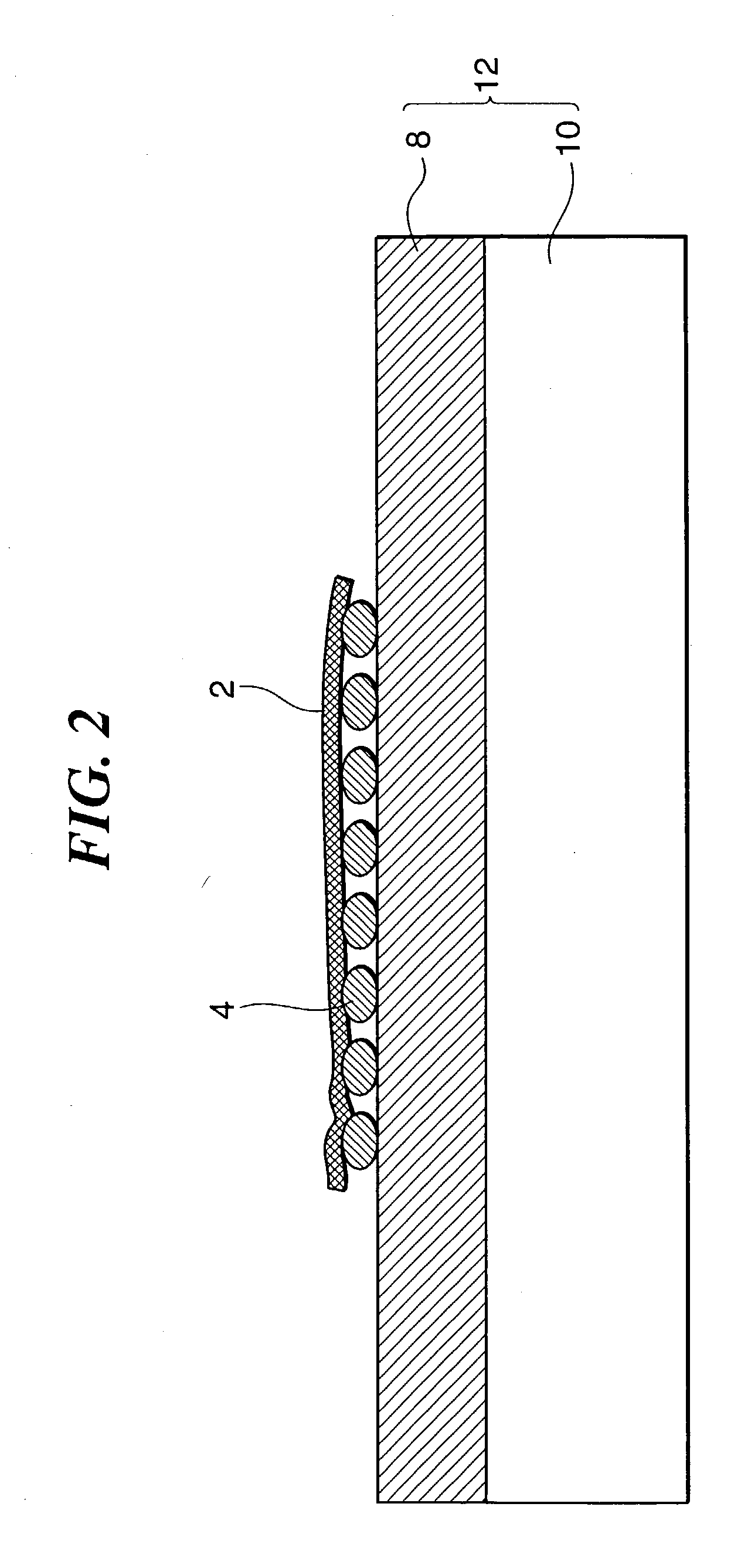
[0099] In this example, the same photoelectric element having the same structure as shown in FIG. 1 was fabricated except that plural carbon nano-tubes were used.
[0100] At first, an S-doped n-type InP substrate ((100 face) sized 20 mm.times.20 mm and with 500 .mu.m in thickness was sputter etched to about 30 nm by an argon beam sputtering method. Subsequently, chemical etching was applied with a solution including H.sub.2SO.sub.4:H.sub.2O:H.-sub.2O.sub.2=3:1:1 (mass ratio) for about 80 seconds (kept at a temperature of 25.degree. C.), the substrate was washed with super purified water, and dried with isopropyl alcohol to form a support plate 10. Then, an undoped InP layer (about 1 .mu.m in thickness) was epitaxially grown by a halogeno chemical vapor deposition method to epitaxially grow an undoped InP layer (about 1 .mu.m in thickness) to form a dispersion elimination layer 8. A parallel electrode pattern (sized 500 .mu.m.times.200 .mu.m) was formed on the dispersion elimination la...
example 2
[0107] In this example, a photoelectric conversion element of the same structure as shown in Example 1, excepting that the material for each of component was different, was fabricated. However, the layer formed on the support plate (quartz substrate) is not a dispersion elimination layer but a silicon nitride layer as a dielectric layer. Further, since adhesion was not sufficient when a gold electrode was intended to be formed directly on the surface of the silicon nitride layer, a Ti layer was put between them as a bonding layer.
[0108] At first, a silicon nitride layer (200 nm in thickness) was grown on one surface of a quartz substrate sized 10 mm.times.10 mm and with 500 .mu.m in thickness by a plasma chemical vapor phase deposition method, to form an uppermost surface layer. Then, a pair of Au electrodes having a Ti layer as an a bonding layer (Ti / Au electrode, Ti layer: 100 nm thickness, gold layer: 300 nm thickness) were formed. A pair of Ti / Au electrodes were formed by an ele...
example 3
[0117] In this example, a photoelectric conversion element of the same structure as in Example 2 was fabricated except for not forming a fine InAs particle layer between the electrodes but using only the carbon nano-tubes as the light sensor. In the same manner as in Example 2, a silicon nitride layer (200 nm in thickness) was grown on a quartz substrate by a plasma chemical vapor phase deposition method, a Ti / Au electrode was formed by an electron beam vapor deposition method and, further, plural single wall carbon nano-tubes each of about 3 nm in diameter fabricated by an arc discharging method were connected between the electrodes in a state of bridging the pair of electrodes.
[0118] The photoelectric conversion element of this example was obtained as described above.
[0119] The thus obtained photoelectric conversion element of this example was incorporated in the same optical system and the measuring system as those in Example 1, and the photoelectric conversion characteristics we...
PUM
 Abstract
Description
Claims
Application Information